Method and correlated device for confirming optimum object plane and optimum image plane of photo-etching projection device

A technology of lithographic projection and projection objective lens, which is applied in the direction of photolithography exposure device, microlithography exposure equipment, etc., can solve the problem that the best image plane or object plane of projection objective lens, and the accuracy of object plane or image plane cannot be guaranteed. and other problems, to achieve the effect of easy online implementation, low cost and high measurement accuracy

Active Publication Date: 2008-05-07
SHANGHAI MICRO ELECTRONICS EQUIP (GRP) CO LTD
View PDF1 Cites 13 Cited by
  • Summary
  • Abstract
  • Description
  • Claims
  • Application Information

AI Technical Summary

Problems solved by technology

However, the position of the image plane or object plane as a fixed position cannot be guaranteed to be the best image plane or object plane of the projection objective lens, so the accuracy of the object plane or image plane obtained by this method cannot be guaranteed

Method used


Image

  • Method and correlated device for confirming optimum object plane and optimum image plane of photo-etching projection device
  • Method and correlated device for confirming optimum object plane and optimum image plane of photo-etching projection device
  • Method and correlated device for confirming optimum object plane and optimum image plane of photo-etching projection device

Examples


Embodiment Construction

[0025] The specific embodiments of the present invention will be further described below in conjunction with the accompanying drawings.

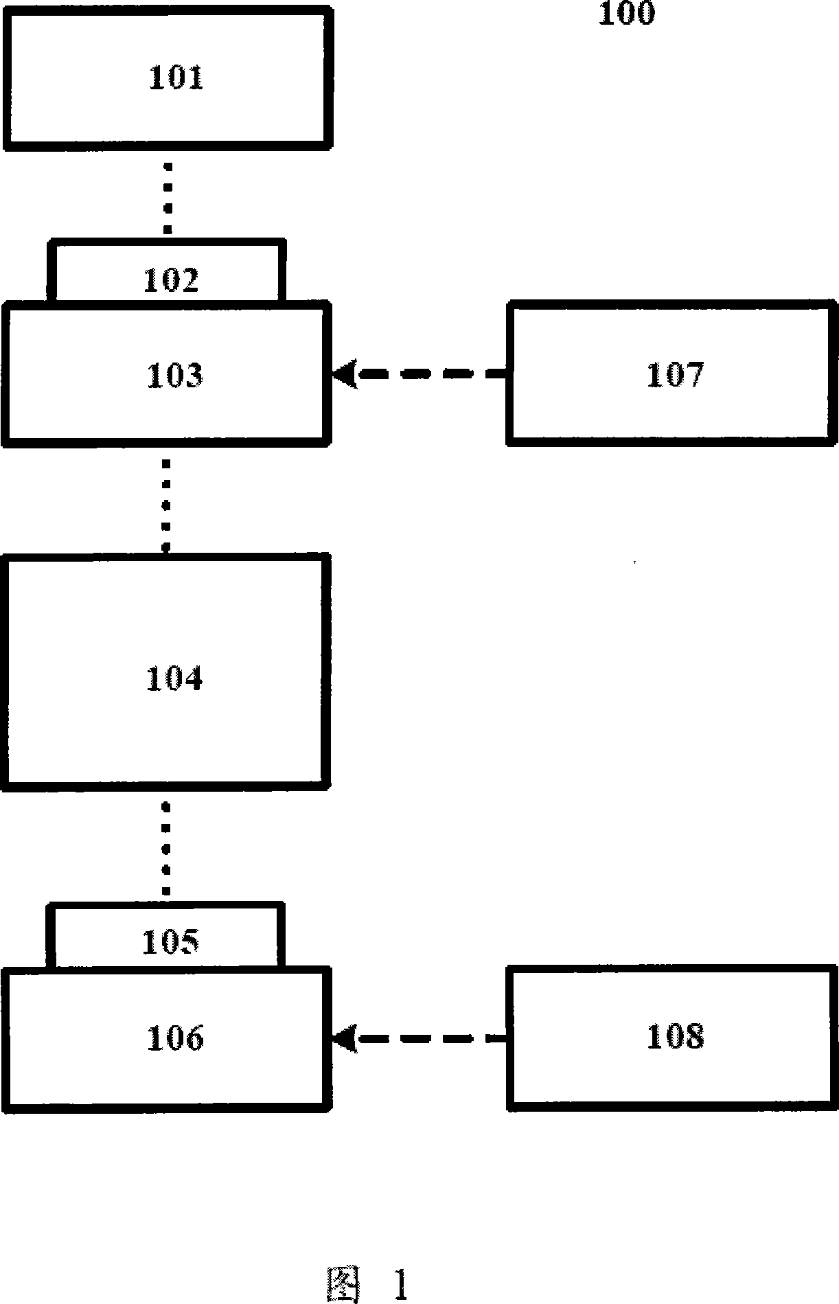
[0026] FIG. 1 is a schematic diagram of the structure of a photolithographic projection device. The lithography projection apparatus 100 includes a light source 101 , a projection objective lens 104 , a mask table 103 and a mask plate 102 thereon, a workpiece table 106 and a wafer 105 thereon. The light source 101 is used to generate a projection light beam. After the projection beam irradiates the mask plate 102 held by the mask table 103 , the circuit pattern on the mask plate 102 is imaged in the photoresist on the upper surface of the wafer 105 through the projection objective lens 104 . After the exposed wafer 105 undergoes a chemical treatment process, the pattern on the mask plate 102 is transferred to the photoresist on the surface of the wafer 105 . The lithography projection apparatus 100 further includes a mask stage motion cont...


PUM


Abstract

The invention discloses a method for determining the optimal object plane and the optimal image surface of a photoetching projecting device, and the relevant device thereof. The invention utilizes a two-dimensional exposure method, namely, the stepping of a mask and a wafer in a certain range is controlled to obtain a group of exposure markers corresponding to the different object plane and optimal image positions on the wafer, the resolution ratio of the groups of exposure markers is compared to determine the position of the optimal object plane and image surface. Compared with the prior art, the precision of the optimal object plane and the optimal image surface obtained by the method is higher, and the cost problem brought in order to provide the high precision in the prior art is solved.

Description

technical field [0001] The invention relates to a photolithography method and a photolithography device, in particular to a method for determining an optimal object plane and an optimal image plane of a photolithography projection device and related devices. Background technique [0002] Photolithography equipment is mainly used in the manufacture of integrated circuits IC or other micro-devices. With a photolithographic apparatus, a mask pattern can be imaged on a photoresist-coated wafer, such as a semiconductor wafer or an LCD panel. The lithography device exposes through the projection objective lens and transfers the designed mask pattern to the photoresist. As the core component of the lithography device, the object plane and mirror position of the projection objective lens have an important impact on the lithography imaging quality. [0003] In order to obtain the best imaging effect, at the time of exposure, the lower surface of the mask pattern must be placed at th...

Claims


Application Information

Patent Timeline
Patent Type & Authority Applications(China)
IPC IPC(8): G03F7/20
Inventor 毛方林
Owner SHANGHAI MICRO ELECTRONICS EQUIP (GRP) CO LTD
Why Eureka
Try Eureka