

Polishing pad and chemico-mechanical polishing method
A chemical machinery, polishing pad technology, applied in surface polishing machine tools, grinding/polishing equipment, electrical components, etc., can solve the problems of difficult to pull out the wafer, the surface of the wafer cannot meet the application requirements, etc., and achieve high surface flatness degree of effect
- Summary
- Abstract
- Description
- Claims
- Application Information
AI Technical Summary
Problems solved by technology
Method used
Image

Examples
Embodiment Construction
[0036] The specific implementation of the present invention will be described in detail below in conjunction with the accompanying drawings and specific embodiments.
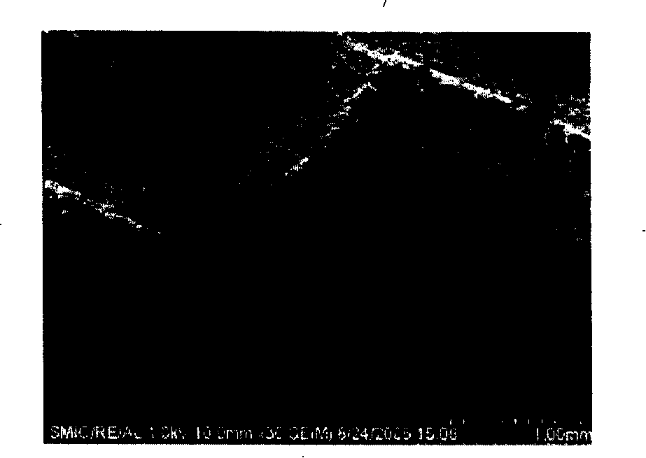
[0037] The polishing pads currently used in the chemical mechanical polishing process are all polishing pads with grooves on the polishing surface. After polishing the wafer with a polishing pad with grooves on the polishing surface, the flatness of the wafer surface cannot be applied to the device used for image transmission. In order to obtain a better flatness on the wafer surface, the present invention studies the reasons for the concaves on the wafer surface after chemical mechanical polishing. Observing the polishing pad with concave parts on the polishing surface through electron microscope, it is found that the microstructure of the concave parts on the polishing surface is as follows: image 3 As shown, the recess can be clearly seen from the figure.
[0038] to have as figure 2 After the polishing ...
PUM
 Abstract
Description
Claims
Application Information