

Circuit connection calibration system and method
A technology of circuit connection and verification method, which is applied in the direction of electrical digital data processing, special data processing applications, instruments, etc., can solve problems such as low work efficiency, time-consuming, delayed completion of circuit pattern layout, etc., to improve the accuracy rate , the effect of reducing the chance of modification
- Summary
- Abstract
- Description
- Claims
- Application Information
AI Technical Summary
Problems solved by technology
Method used
Image

Examples
Embodiment Construction
[0029] Embodiments of the present invention are described below through specific examples, and those skilled in the art can easily understand other advantages and effects of the present invention from the content disclosed in this specification. The present invention can also be implemented or applied through other different specific examples, and various modifications and changes can be made to the details in this specification based on different viewpoints and applications without departing from the spirit of the present invention.
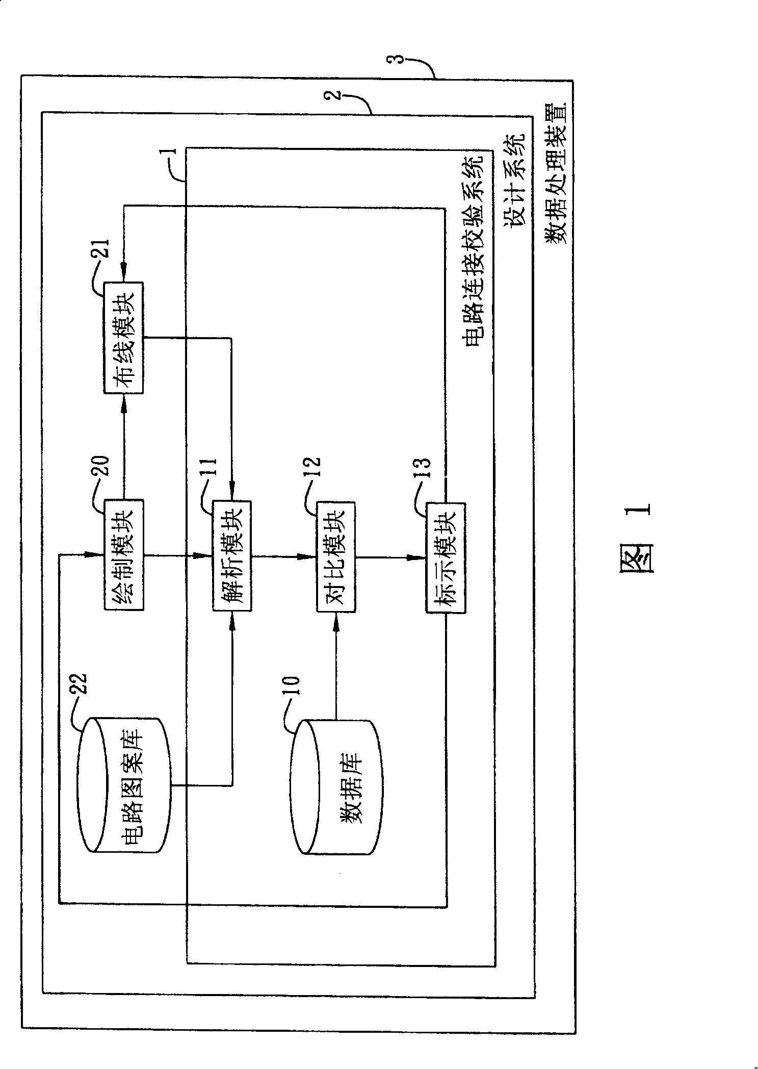
[0030] Please refer to FIG. 1 , which is a schematic diagram of the application architecture of the circuit connection verification system of the present invention. It should be noted that the circuit connection verification system 1 of the present invention may include other components. To simplify the drawings and descriptions, the basic structure here only shows components related to the present invention.
[0031] In this embodiment, the cir...
PUM
 Abstract
Description
Claims
Application Information