Circuit board structure and its making method

A manufacturing method and circuit board technology, which are applied in multilayer circuit manufacturing, printed circuit components, and electrical connection printed components, etc., can solve the problems of difficult control of wire thickness, difficult definition of line width, and inability to achieve, so as to improve reliability. and quality, control thickness, improve the effect of adhesion

Inactive Publication Date: 2008-06-04
UNIMICRON TECH CORP
View PDF0 Cites 23 Cited by
  • Summary
  • Abstract
  • Description
  • Claims
  • Application Information

AI Technical Summary

Problems solved by technology

However, the above-mentioned resist layer is limited by the manufacturing method capabilities such as exposure and development or laser opening precision, and the adhesion of the conductive layer, such as the limitation of the wavelength of ultraviolet light used, and the photoresist pattern at the edge part becomes blurred due to diffraction during exposure. , so the line width is not easy to define, and it is impossible to achieve a thinner line width, and at the same time it makes the thickness of the wire difficult to control

Method used


Image

  • Circuit board structure and its making method
  • Circuit board structure and its making method
  • Circuit board structure and its making method

Examples


Embodiment Construction

[0039] Embodiments of the present invention are described below through specific specific examples, and those skilled in the art can easily understand other advantages and technical effects of the present invention from the content disclosed in this specification.

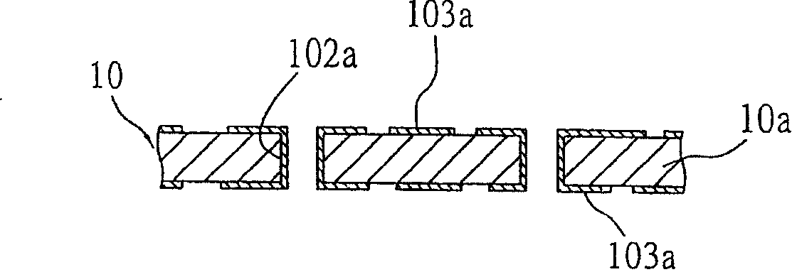
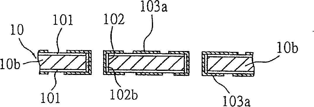
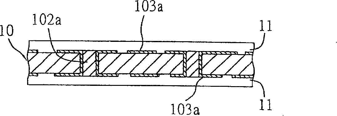
[0040] Such as Figure 1A to Figure 1H Shown is a schematic cross-sectional view of the first embodiment of the manufacturing method of the circuit board structure of the present invention in detail. It should be noted that the above-mentioned figures are all simplified schematic diagrams, and only schematically illustrate the manufacturing method of the circuit board of the present invention. However, said figure only shows components related to the present invention, and the components shown are not in the form of actual implementation. The number, shape and size ratio of components in actual implementation are a kind of selective design, and the layout of the components Forms can be more complex.

[0041] see ...


PUM


Abstract

The invention relates to a structure of a circuit wafer and a making method thereof, mainly providing a surface which has at least a base body of a first circuit layer; a dielectric layer is formed on the surface of the base body, and a plurality of openings of a first and a second types are formed in the dielectric layer, wherein the openings of the second type are used for exposing an electrical connection pad of the first circuit layer; then a metal layer is formed on the surface of the dielectric layer and in the openings of the first and second types; and the metal layer on the surface of the dielectric layer is removed to form a second circuit layer in the opening of the fist type of the dielectric layer; then electricity is formed in the openings of the second type to connect with the structure of electric conduction in the first circuit layer, thus strengthening adhesion between the circuit and the dielectric layer and increasing the ability of making thin circuit in the circuit wafer.

Description

technical field [0001] The invention relates to a circuit board structure and a manufacturing method thereof, in particular to a manufacturing method of a build-up circuit board with thin lines. Background technique [0002] With the vigorous development of the electronic industry, electronic products are gradually stepping into the research and development trend of multi-function and high performance. In order to meet the packaging requirements of high integration and miniaturization of semiconductor packages for more active and passive components and circuit loading, semiconductor packaging substrates have gradually evolved from double-layer circuit boards to multi-layer circuit boards ( Multi-layerboard), so that the interlayer connection technology (Interlayer connection) can be used in a limited space to expand the available circuit layout area on the semiconductor packaging substrate, thereby meeting the needs of integrated circuits with high circuit density and reduci...

Claims


Application Information

Patent Timeline
Patent Type & Authority Applications(China)
IPC IPC(8): H05K3/46H05K1/11
Inventor 许诗滨颜雅仑
Owner UNIMICRON TECH CORP
Why Eureka
Try Eureka