Defect testing device and method

A defect inspection and defect technology, applied in measurement devices, image enhancement, instruments, etc., to achieve the effect of improving productivity and making it easier to judge whether it is qualified or not.

Inactive Publication Date: 2008-06-11
OLYMPUS CORP
View PDF3 Cites 32 Cited by
  • Summary
  • Abstract
  • Description
  • Claims
  • Application Information

AI Technical Summary

Problems solved by technology

In the technology described in Patent Document 1, in order to expand the dynamic range of the intensity of scattered light from foreign objects, inspection is performed under two inspection conditions and the inspection results are integrated, but this does not directly contribute to making pass / fail judgment easier Methods

Method used


Image

  • Defect testing device and method
  • Defect testing device and method
  • Defect testing device and method

Examples


Embodiment Construction

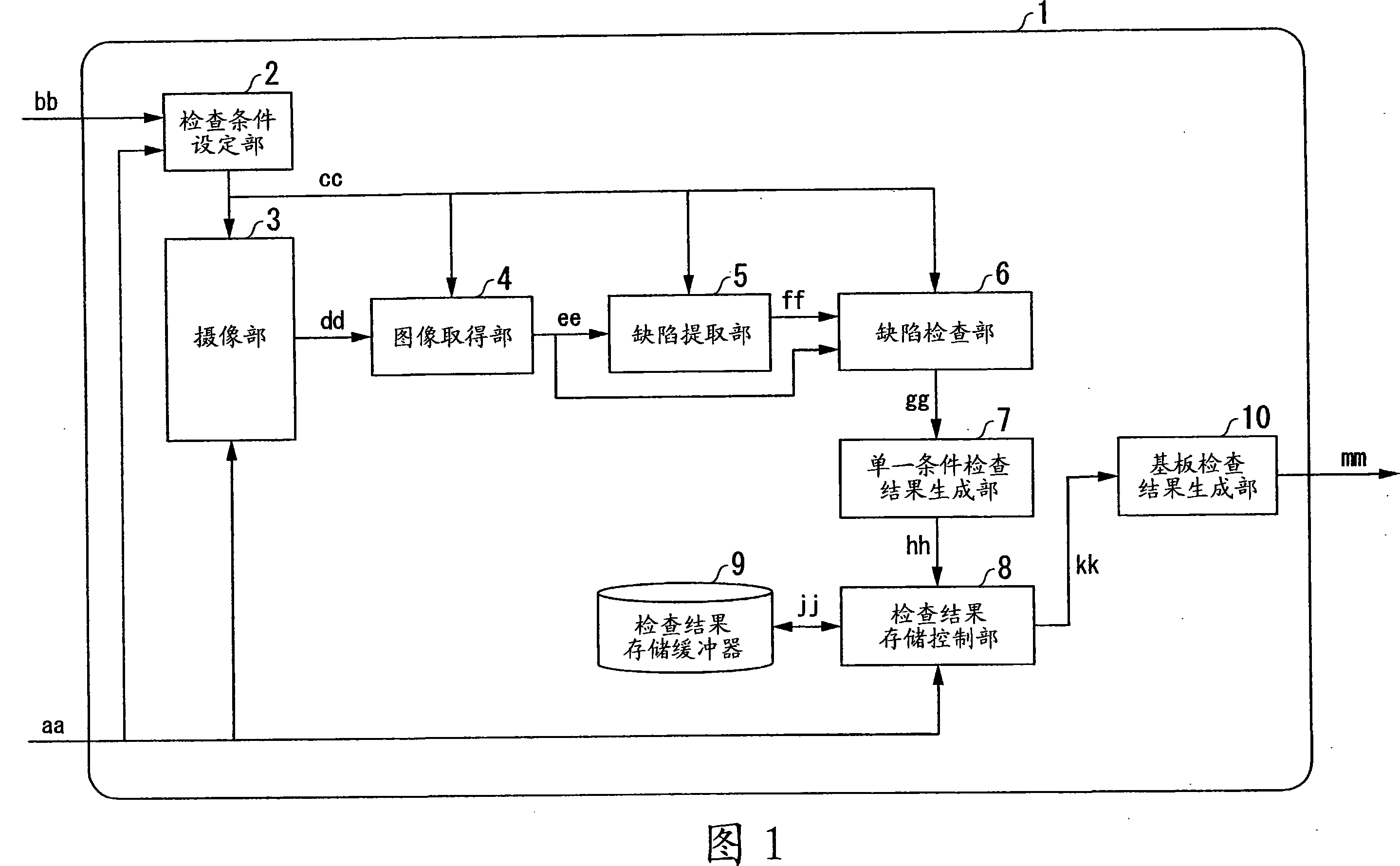
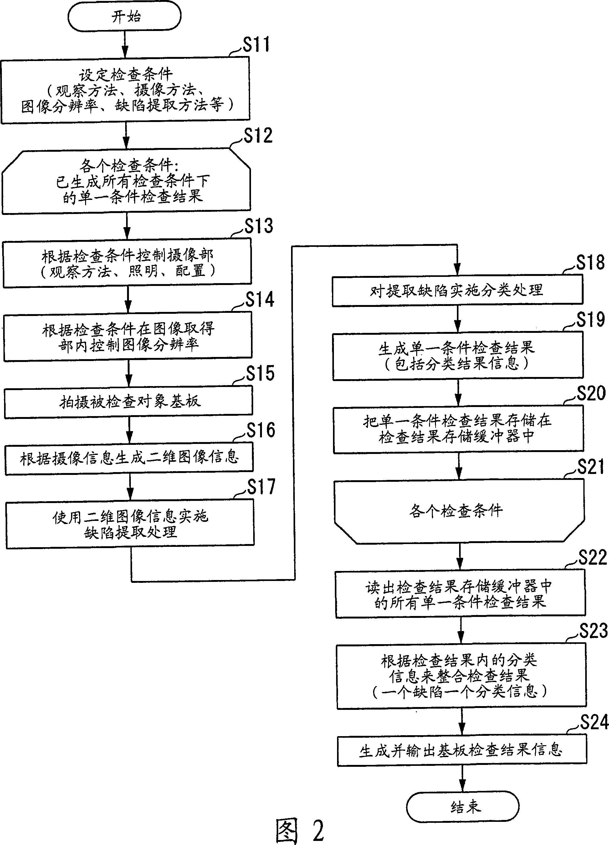
[0027] Hereinafter, embodiments of the present invention will be described with reference to the drawings. In this embodiment mode, the present invention is applied to an inspection device for macroscopic inspection of a semiconductor wafer. FIG. 1 shows the configuration of an inspection device according to this embodiment. The inspection device 1 receives the control information aa for the control device, and related information indicating the substrate to be inspected (object to be inspected) (indicating the model number, process of the substrate, and the size and position of the chip and the exposure shot area (shot). The board information bb of design information, etc.) is used as input information from the outside. On the other hand, the inspection apparatus 1 outputs inspection result information mm related to an inspection target substrate as output information to the outside.

[0028] The control information aa and substrate information bb input into the inspection ...


PUM


Abstract

The invention provides a defect inspection device and a defect inspection method. An imaging unit (3) images an object to be inspected to generate imaging information. An image generating unit (4) generates an image of an object to be inspected based on imaging information. A defect extraction unit (5) extracts defects on the object to be inspected using the generated image. A defect inspection unit (6) inspects the extracted defects and generates inspection results for each inspection condition. The inspection result generation unit (10) weights the inspection results under each inspection condition according to the defect-related information, and integrates the inspection results under each inspection condition on this basis. Accordingly, it is possible to provide a defect inspection device and a defect inspection method capable of improving the productivity of the entire manufacturing process by facilitating the pass / fail judgment of the substrate.

Description

technical field [0001] The present invention relates to a method for inspecting substrates and semiconductor wafers for FPDs (Flat Panel Displays) such as LCDs (Liquid Crystal Displays) and PDPs (Plasma Display Panels) as inspected objects. Defect inspection device and defect inspection method. [0002] This application claims priority from prior Japanese Patent Application No. 2006-331770 filed on December 8, 2006, the contents of which are incorporated herein by reference. Background technique [0003] In the above-mentioned inspection of the substrate, the inspection is carried out according to various conditions in one inspection device, and as the inspection result under each inspection condition, information on the presence or absence of defects and characteristic information (position, area, etc.) Pass / fail judgment results of predetermined areas (chips in semiconductor wafers, panels in FPD, etc.), etc. There are characteristics in the inspection of each inspection...

Claims


Application Information

Patent Timeline
Patent Type & Authority Applications(China)
IPC IPC(8): H01L21/66H01J9/42G02F1/13G01N21/956
CPCG06T2207/30121G01N21/95607G09G3/006G01N2021/9513G01N21/9501G06T2207/30148G06T7/001G06T7/0006G01N2021/8825
Inventor 堀内一仁
Owner OLYMPUS CORP
Why Eureka
Try Eureka