III-V family metal oxide semiconductor luminous fieldistor and method for producing the same

A field effect transistor and oxide semiconductor technology, applied in the field of III-V metal oxide semiconductor light emitting field effect transistor and its preparation, can solve the problem of low luminous efficiency of the light emitting transistor, and achieve convenient control, high luminous efficiency, high luminous efficiency and the like. effect of brightness

Inactive Publication Date: 2008-06-11
SOUTH CHINA NORMAL UNIVERSITY
View PDF0 Cites 10 Cited by
  • Summary
  • Abstract
  • Description
  • Claims
  • Application Information

AI Technical Summary

Problems solved by technology

[0003] The object of the present invention is to provide a III-V metal oxide semiconductor light-emitting field-effect transistor with high luminous e

Method used


Image

  • III-V family metal oxide semiconductor luminous fieldistor and method for producing the same

Examples


Embodiment

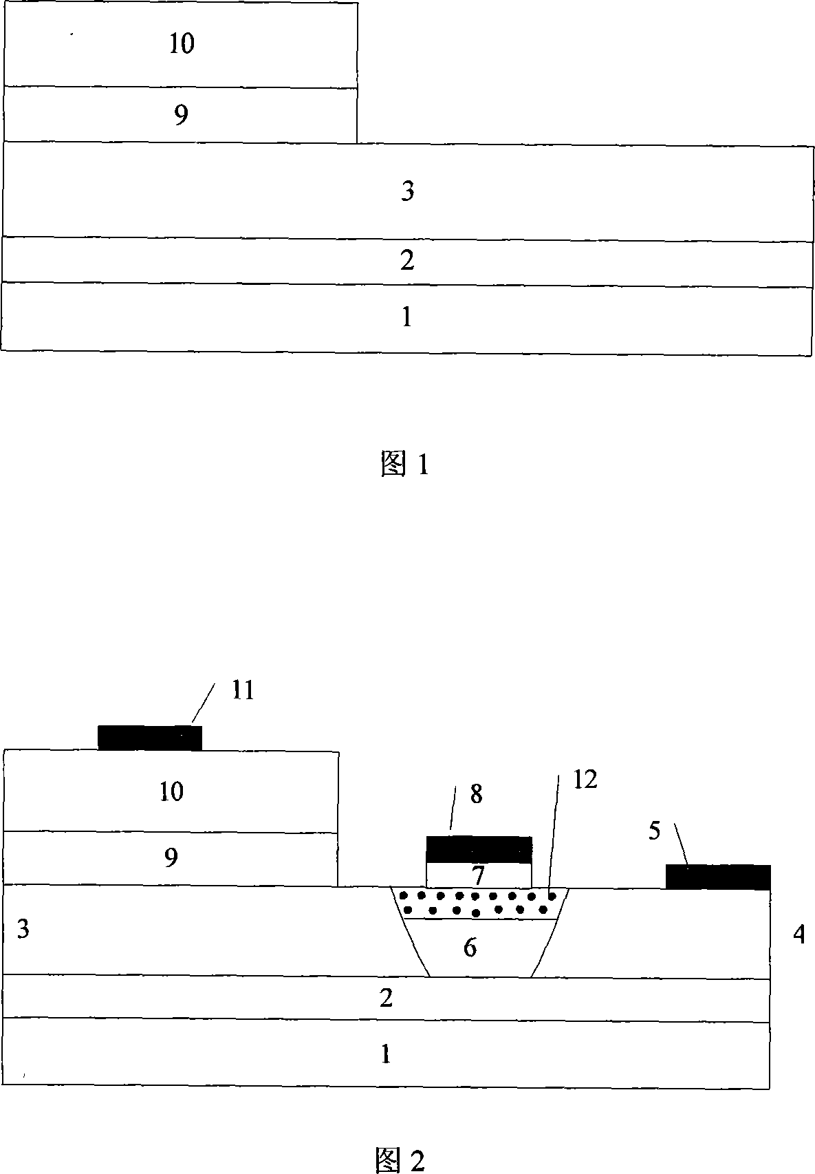
[0025] The MOS field effect transistor is prepared by using III-V compound material GaN material. A MOS type light emitting field effect transistor adopts a sapphire substrate and is composed of a source, a gate, an active light emitting region and a drain. Form a buffer layer 2 on a sapphire material substrate 1, then form an n-type semiconductor layer 3, continue to grow a multi-quantum well active light-emitting layer 9 and a p-type doped drain region 10, and finally form an epitaxial wafer. Then the semiconductor layer 3 is etched to form a step structure, and the left region of the step adopts an ion implantation method to manufacture a p-type semiconductor gate region 6, and then MgO is deposited on the p-type gate region 6 as a gate oxide layer 7 and a gate metal electrode 8, The right end of the n-type semiconductor layer 3 is the n-type source region 4 , on the n-type source region 4 is the source electrode 5 , and the drain region ohmic contact drain 11 .

[0026] T...


PUM


Abstract

The invention discloses a III-V group metal oxide semiconductor type luminescent field effect transistor (FET) and a method for preparing the same, wherein the FET comprises a p-type drain region, an active area, an n-type semiconductor layer, a buffer layer and a substrate which are stacked in turn in vertical direction; a p-type gate region is arranged at the left side of the transverse step structure of the n-type semiconductor layer, while an n-type source region is arranged at the right side of the step structure; a grid electrode oxidation layer and a grid electrode are stacked on the p-type gate region; an electronic channel, which is formed by a MOS structure on the surface of a gate region semiconductor, is arranged between the p-type gate region and the grid electrode oxidation layer; the n-type source region is provided with a source electrode, while the p-type drain region is provided with a drain electrode. The transverse structure of the step of the invention is used to control the luminous intensity of a device by means of metal-oxide-semiconductor contact field effect, while the vertical structure is used to generate recombination luminescence; moreover, the structure has high luminous efficiency and high brightness and is convenient for control.

Description

technical field [0001] The invention relates to a III-V group metal oxide semiconductor light-emitting field-effect transistor and a preparation method thereof. Background technique [0002] In the prior art, the basic structure of a light emitting diode (LED) is composed of a p-type electrode, an active light-emitting region and an n-type electrode. Connect the p-terminal and n-terminal of the LED into the circuit, supply power through a constant current source, and adjust the terminal voltage of the LED to control the luminous intensity of the LED. At present, the manufacturing technology of light-emitting transistors is not yet mature, and is still in the initial research stage. The main methods are: one is an NPN light-emitting transistor device manufactured according to the traditional transistor principle, which not only uses the p-type doped region of the device to emit light, but also controls it as a base region. However, because the base region is very thin, most ...

Claims


Application Information

Patent Timeline
IPC IPC(8): H01L33/00
Inventor 郭志友张建中孙慧卿尉然范广涵
Owner SOUTH CHINA NORMAL UNIVERSITY
Why Eureka
Try Eureka