SCR electrostatic protection device and method of manufacture

A technology of electrostatic protection and devices, which is applied in the field of semiconductor electrostatic protection, can solve the problems that the protection ability cannot be fully exerted, and the opening voltage of silicon controlled rectifiers is high, so as to achieve the effect of easy opening and lower opening voltage

Inactive Publication Date: 2008-06-18
SHANGHAI HUA HONG NEC ELECTRONICS
View PDF0 Cites 9 Cited by
  • Summary
  • Abstract
  • Description
  • Claims
  • Application Information

AI Technical Summary

Problems solved by technology

[0003] The technical problem to be solved by the present invention is to provide an SCR electrostatic protection device and its manufacturing method, which can solve the problem that the protection ability cannot be fully exerted due to the high turn-on voltage of the silicon controlled rectifier

Method used


Image

  • SCR electrostatic protection device and method of manufacture
  • SCR electrostatic protection device and method of manufacture
  • SCR electrostatic protection device and method of manufacture

Examples


Embodiment

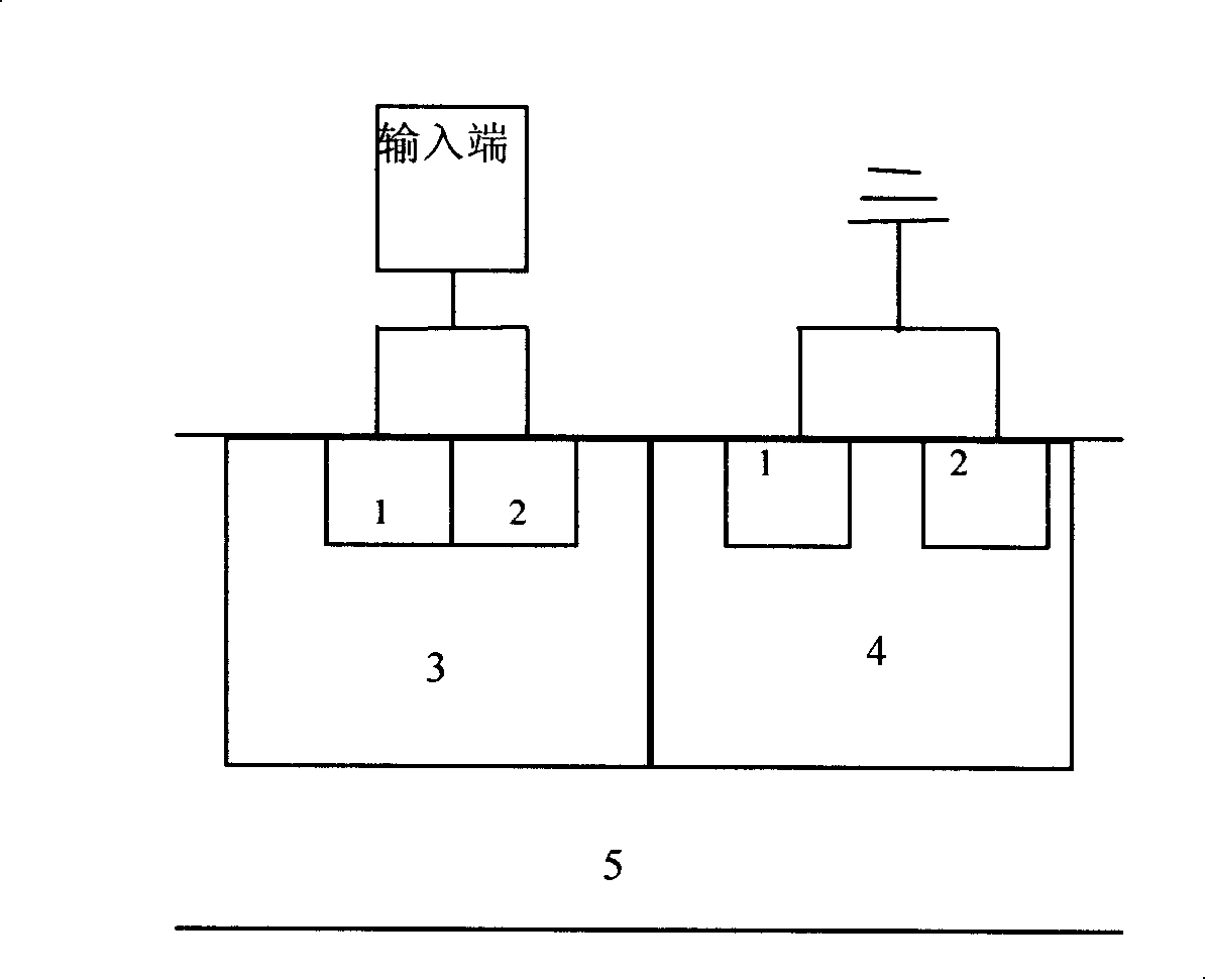
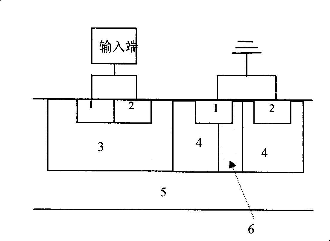
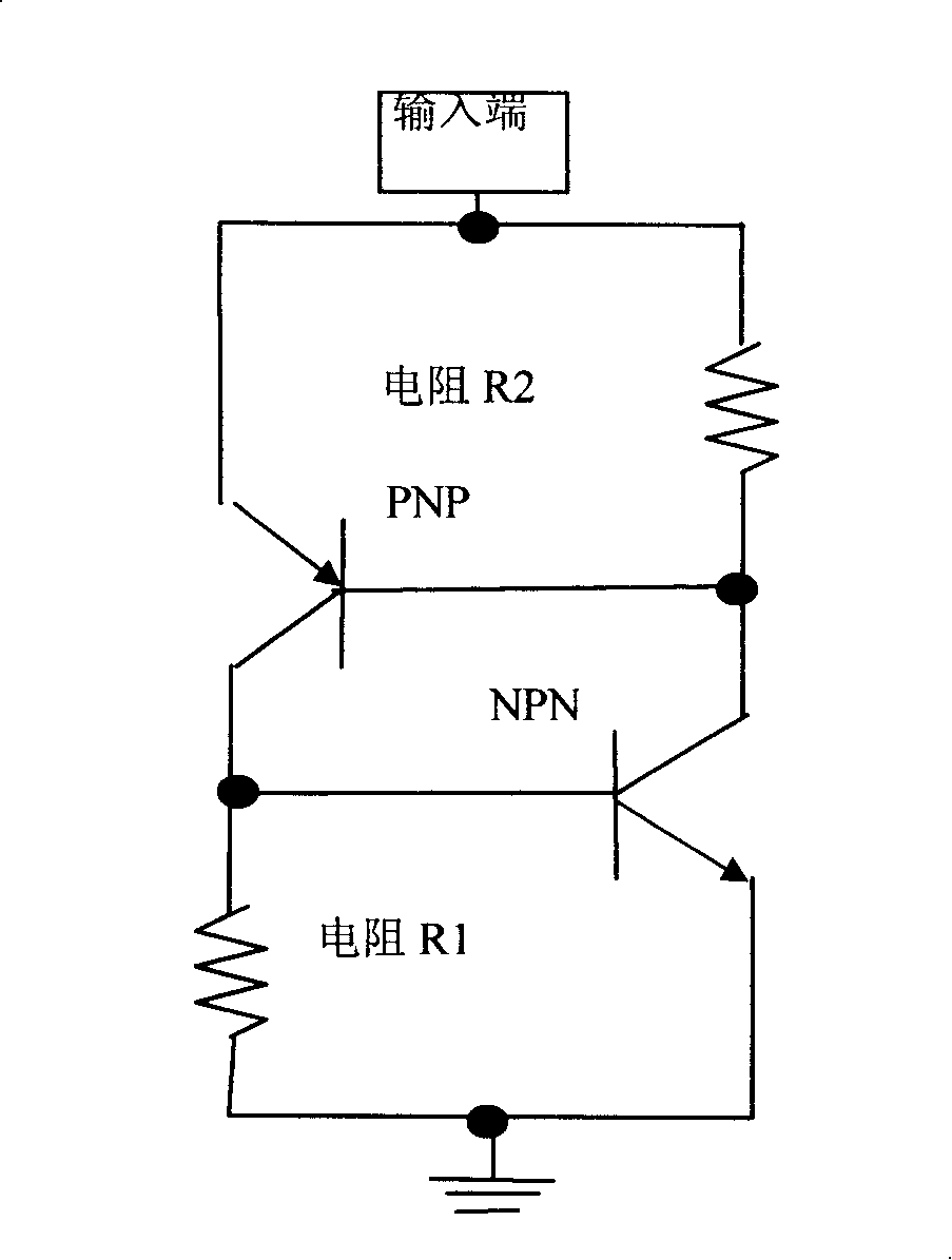
[0014] Such as figure 2 As shown, it is a structural schematic diagram of a specific embodiment of the present invention, wherein: 1 is an N-type implanted region, 2 is a P-type implanted region, 3 is an N-well implanted region, 4 is a P-well implanted region, and 5 is a P-type substrate , 6 is the edge N well region (N well implantation region). In this embodiment, the SCR still includes a P-N-P-N four-layer semiconductor structure, but considering the above-mentioned invention principle, this embodiment is figure 1 After the N-type (N+) implantation region in the shown P well (PWell) is added with an edge N well implantation region (Nwell), image 3 The resistance of the shown substrate resistance R1 will increase, which will make the SCR structure in the embodiment easier to trigger without affecting its protection capability. Therefore, compared with the traditional SCR structure, a better electrostatic protection effect can be obtained. It should be pointed out that t...


PUM


Abstract

The invention discloses an SCR electrostatic protection device and the manufacturing method thereof. The structure of the device comprises a P-type injection region (2) in a P well (4), an N-type injection region (1) in the P well (4), a P-type injection region (2) in an N well (3) and an N-type injection region (1) in the N well (3), and the N-type injection region in the P well (4) is added with a peripheral injection region (6) of N well. Because the invention is added with the peripheral N well region (the injection region of the N well) on the basis of traditional silicon controlled rectifier structure, the invention can reduce the turn-on voltage of the silicon controlled rectifier effectively without affecting the protection ability. Without adding new process condition, parasitic NPN and PNP which are used in ESD discharging can be started more easily, thus fully exerting the capacity of ESD.

Description

technical field [0001] The invention relates to a semiconductor electrostatic protection technology, in particular to an SCR (Silicon Controlled Rectifier, silicon controlled rectifier) ​​electrostatic protection device and a manufacturing method thereof. Background technique [0002] At present, SCR is widely used as an electrostatic discharge (ESD, Electrostatic Discharge) protection device in semiconductor electrostatic protection. Such as figure 1 As shown, it is a schematic structural diagram of a commonly used SCR, which consists of a P-type implanted region in a P-well, an N-type implanted region in a P-well, a P-type implanted region in an N-well, and an N-type implanted region in an N-well. P-N-P-N Four-layer semiconductor structure. image 3 is the equivalent circuit of the commonly used SCR above, such as image 3 As shown, the coupling of parasitic NPN and parasitic PNP transistors will be formed, and when static electricity arrives and reaches a certain volta...

Claims


Application Information

Patent Timeline
Patent Type & Authority Applications(China)
IPC IPC(8): H01L27/04H01L23/60
CPCH01L29/87
Inventor 徐向明苏庆
Owner SHANGHAI HUA HONG NEC ELECTRONICS
Why Eureka
Try Eureka