Self-aligning metal silicide preparation method

A metal silicide and manufacturing method technology, applied in semiconductor/solid-state device manufacturing, electrical components, circuits, etc., can solve problems such as poor thickness uniformity of metal silicide, achieve good consistency, improve stability, and improve the process window Effect

Inactive Publication Date: 2008-07-02
SEMICON MFG INT (SHANGHAI) CORP
View PDF1 Cites 14 Cited by
  • Summary
  • Abstract
  • Description
  • Claims
  • Application Information

AI Technical Summary

Problems solved by technology

[0008] Therefore, the object of the present invention is to provide a method for manufacturing salicide, to solve the problem of poor thickness uniformity of the metal silicide formed by the existing method

Method used


Image

  • Self-aligning metal silicide preparation method
  • Self-aligning metal silicide preparation method
  • Self-aligning metal silicide preparation method

Examples


Embodiment Construction

[0036] In order to make the above objects, features and advantages of the present invention more comprehensible, specific implementations of the present invention will be described in detail below in conjunction with the accompanying drawings.

[0037] Figure 4 It is a flow chart of the first embodiment of the method for manufacturing a salicide of the present invention.

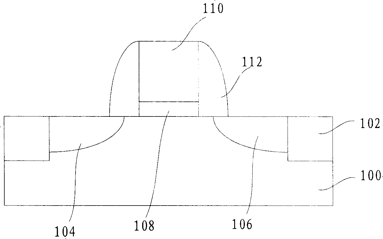
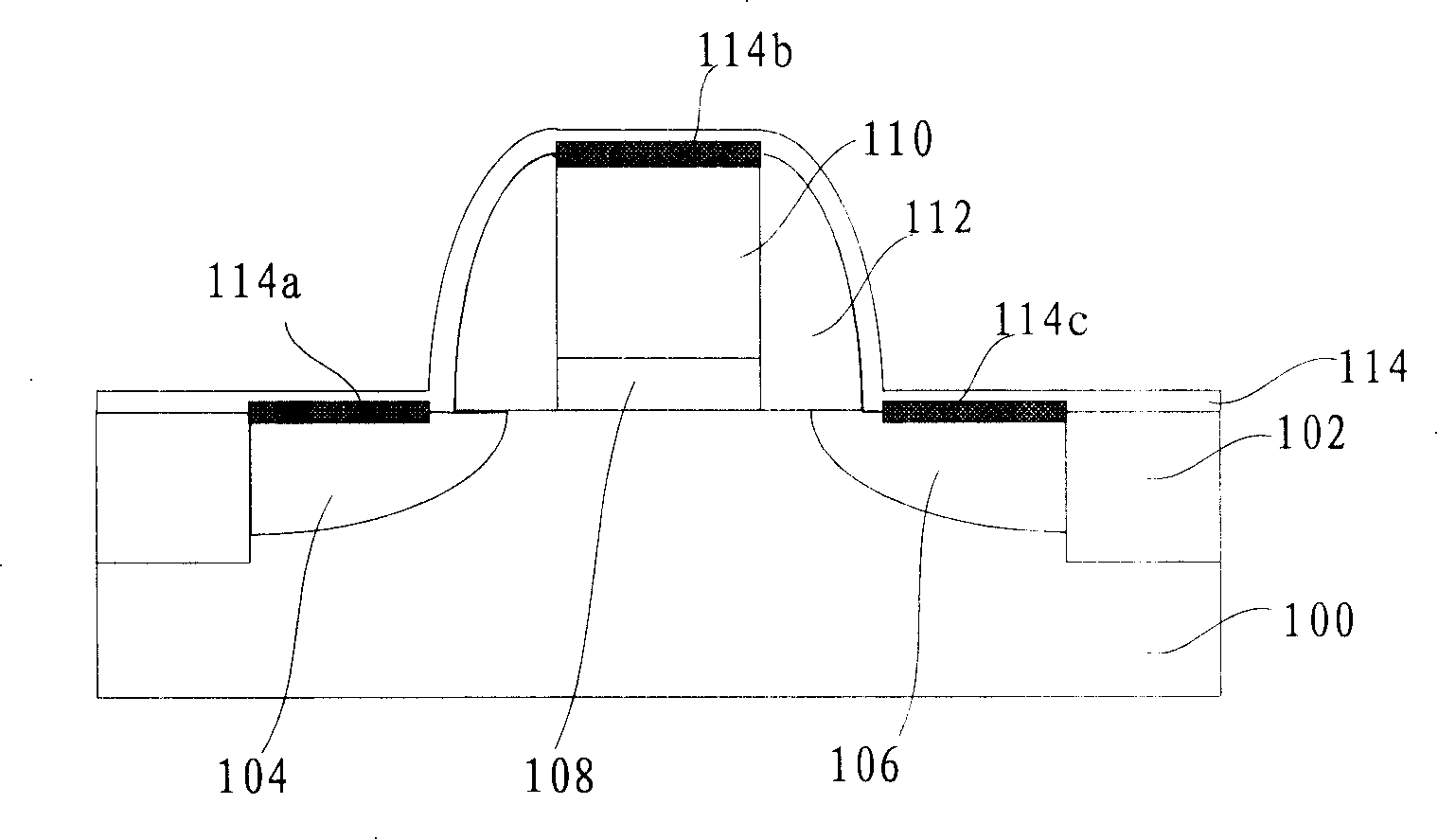
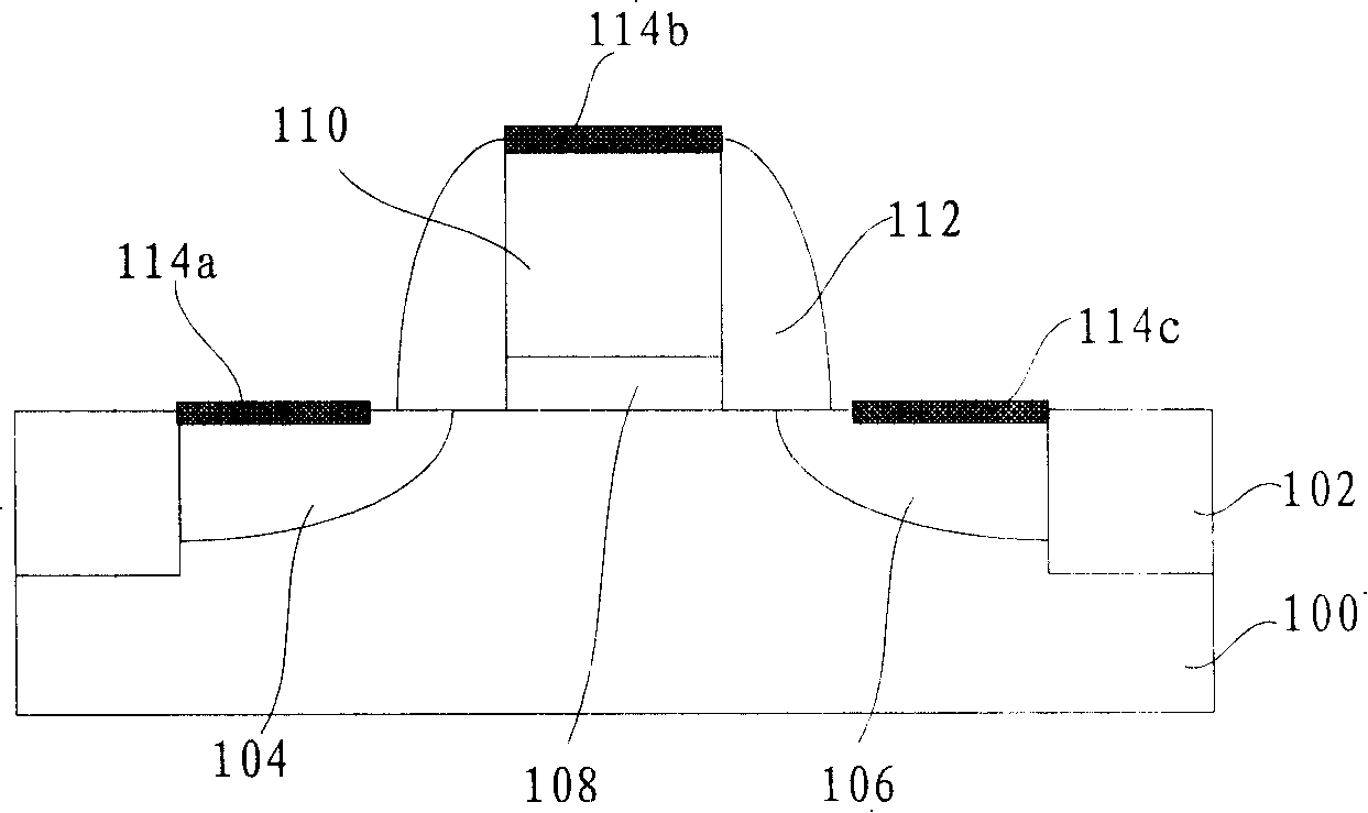
[0038] Such as Figure 4 As shown, a semiconductor substrate is provided, and at least one silicon region is provided on the surface of the semiconductor substrate (S200). In this embodiment, a semiconductor substrate including a metal-oxide-semiconductor transistor is taken as an example. The metal-oxide-semiconductor transistor includes a source, a drain, and a gate, and sidewall protection layers are formed on both sides of the gate. The sidewalls may be one of silicon oxide, silicon nitride or a combination thereof. An isolation trench is formed in the semiconductor base, and silicon oxide is filled ...


PUM


Abstract

A method for manufacturing a self-aligned metal silicide comprises the steps that: a semiconductor substrate is provided and at least a silicon area is arranged on the surface of the semiconductor substrate; a metal layer is formed on the semiconductor substrate and the first step of annealing process is applied to the semiconductor substrate and the second step of annealing process is applied to the semiconductor substrate; the metal layer is removed by etching. The thickness and resistivity of the metal silicide formed through the method of the invention have better consistence.

Description

technical field [0001] The invention relates to the technical field of semiconductor manufacturing, in particular to a method for manufacturing a self-aligned metal silicide. Background technique [0002] Metal silicide is widely used in source-drain contacts and gate contacts to reduce contact resistance due to its low resistivity and good adhesion to other materials. The refractory metal and silicon react together to form a metal silicide, and a low-resistivity metal silicide can be formed through a one-step or multi-step annealing process. With the shrinking of the size of semiconductor devices, the requirements for device performance are getting higher and higher, especially for technology nodes of 90nm and below. In order to obtain lower contact resistance, the industry uses nickel, cobalt and other metals instead of titanium to form low resistivity. metal silicide metal material. Chinese patent application No. 03814954.0 discloses a method for manufacturing nickel me...

Claims


Application Information

Patent Timeline
Patent Type & Authority Applications(China)
IPC IPC(8): H01L21/321H01L21/28H01L21/768
Inventor 朱津泉周祖源
Owner SEMICON MFG INT (SHANGHAI) CORP
Why Eureka
Try Eureka