Mixed microstrip line device for suppressing electromagnetic radiation of dual-band mobile telephone
A technology of electromagnetic radiation and microstrip line, which is applied to the structure of radiation elements, antennas, electrical components, etc., and can solve problems such as electromagnetic radiation and excessive mobile phone calls.
- Summary
- Abstract
- Description
- Claims
- Application Information
AI Technical Summary
Problems solved by technology
Method used
Image

Examples
Embodiment 1
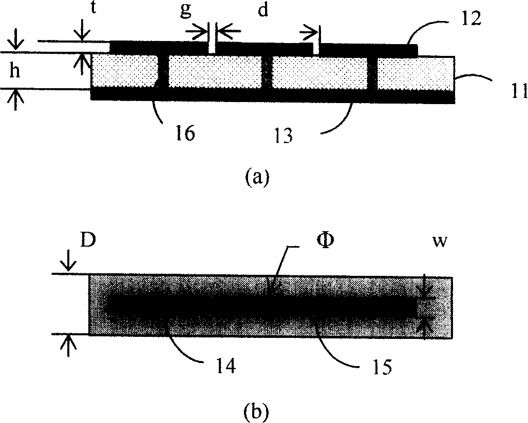
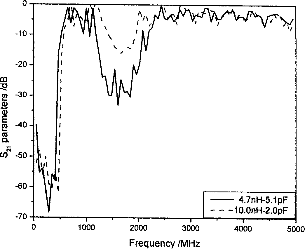
[0022] Metal copper is formed on the surface of the microwave substrate by etching or printing techniques to complete the production of left / right hand mixed microstrip lines. The specific preparation process is as described in the embodiment. The relevant parameters of the microstrip line are set as: h=1.50mm, ε=4.65 (epoxy resin glass cloth), d=8.00mm, g=0.90mm, w=2.80mm, n=8, t=0.018mm, Φ = 1.50mm and D = 8.80mm. A series of chip inductors with package number 0603 L L Welded between the metal conduction strip and the metal grounding plate in parallel; at the same time, a series of chip capacitors C with package number 0805 L Connected in series between adjacent metal conduction strips, the two ends of the chip capacitor are respectively welded to the ends of the two sections of conduction strips, and assembled just above the gap. Depend on image 3 Shown, C L =5.1pF, L L =4.7nH The combined left / right hand hybrid microstrip line has an extremely wide stop band in the f...
Embodiment 2
[0024] Similar to Example 1, metal copper is formed on the surface of the microwave substrate by etching or printing techniques to complete the production of the left / right hand mixed microstrip line, and the specific preparation process is as described in the embodiment. The relevant parameters of the microstrip line are set as: h=1.50mm, ε=4.65 (epoxy resin glass cloth), d=8.00mm, g=0.90mm, w=2.80mm, n=8, t=0.018mm, Φ = 1.50mm and D = 8.80mm. A series of chip capacitors C with package number 0805 L Connected in series between adjacent metal conduction strips, the two ends of the chip capacitor are respectively welded to the ends of the two sections of conduction strips, just above the gap; at the same time, a series of chip inductors with package number 0603 L L Soldered in parallel between the metal conductive strip and the metal ground plate. still by image 3 Know, C L =2.0pF, L L =10.0nH The combined left / right hand mixed microstrip line has a wide stop band in the ...
Embodiment 3
[0026] Metal copper is formed on the surface of the microwave substrate by etching or printing techniques. The specific preparation process is as described in the embodiment. The basic structural unit used in this embodiment is a microstrip line loaded with chip inductors only. The relevant parameters of the microstrip line are set as: h=1.50mm, ε=4.65 (epoxy glass cloth), d=6.00mm, g=0.80mm, w=2.80mm, n=6, t=0.018mm, Φ = 1.50mm and D = 8.80mm. A series of package numbers are 0603, L L =1.0nH chip inductors are soldered in parallel between the metal copper conductive strip and the ground plate. SMD inductor L L 1.8nH, 2.2nH can also be used. Figure 4 It is the microwave transmission curve of the microstrip line loaded with chip inductors. It can be seen from the figure that for the inductances of 1.0nH, 1.8nH and 2.2nH, the electromagnetic band gap less than -50dB appears in the frequency band below 2000MHz, which can completely cover the mobile phone. Dual frequency work...
PUM
 Abstract
Description
Claims
Application Information
 - R&D
- Intellectual Property
- Life Sciences
- Materials
- Tech Scout
- Unparalleled Data Quality
- Higher Quality Content
- 60% Fewer Hallucinations
Browse by: Latest US Patents, China's latest patents, Technical Efficacy Thesaurus, Application Domain, Technology Topic, Popular Technical Reports.
© 2025 PatSnap. All rights reserved.Legal|Privacy policy|Modern Slavery Act Transparency Statement|Sitemap|About US| Contact US: help@patsnap.com