Etching terminal checking device and method for plasma etching equipment

An etching equipment and endpoint detection technology, which is applied in semiconductor/solid-state device testing/measurement, electrical components, semiconductor/solid-state device manufacturing, etc., can solve the problems of high cost of testing equipment, difficulty in software integration and development, CCD stability, Problems such as signal noise and insufficient sensitivity can ensure the normal silicon wafer processing process, ensure the quality of silicon wafer processing, and improve production efficiency.

Active Publication Date: 2008-07-16
BEIJING NAURA MICROELECTRONICS EQUIP CO LTD
View PDF0 Cites 27 Cited by
  • Summary
  • Abstract
  • Description
  • Claims
  • Application Information

AI Technical Summary

Problems solved by technology

[0007] Although this method can capture the end point of the etching process more accurately, the cost of the detection equipment is very high and requires separate data processing software, which makes software integration and development difficult. , signal to noise, and sensitivity are deficient

Method used


Image

  • Etching terminal checking device and method for plasma etching equipment
  • Etching terminal checking device and method for plasma etching equipment
  • Etching terminal checking device and method for plasma etching equipment

Examples


Embodiment Construction

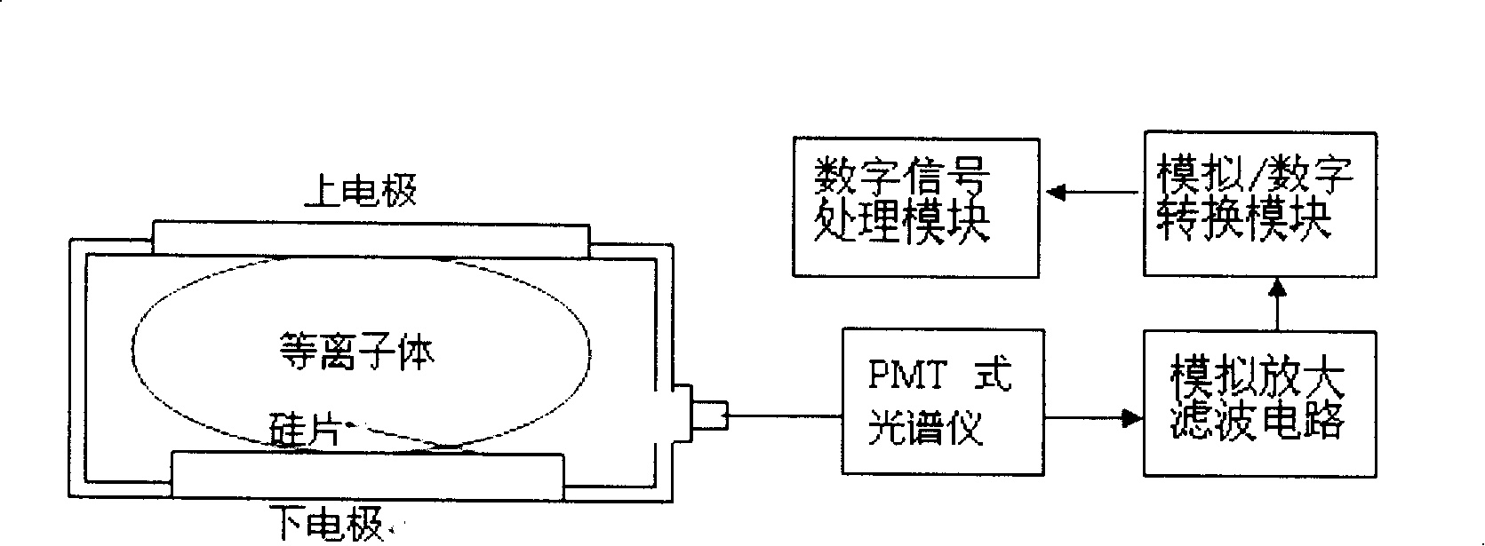
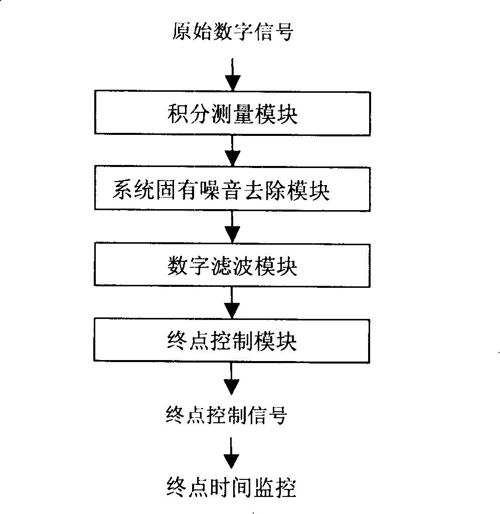
[0030] The etching terminal detection device of a plasma etching equipment according to the present invention, its specific implementation method is as follows figure 1 As shown, it includes a spectrometer, an analog amplification and filtering circuit, an analog / digital conversion module and a digital signal processing module, wherein,

[0031] The spectrometer converts the detected optical signal inside the plasma etching equipment into an analog electrical signal output; the spectrometer is a photomultiplier tube PMT spectrometer, and the PMT receives the spectrum emitted by the plasma in the plasma etching equipment and converts the light The signal is converted into an analog electrical signal. Specifically, during the etching process, the spectrum emitted by the plasma in the reaction chamber of the plasma etching equipment is received by the photomultiplier tube of the PMT spectrometer, and the light intensity change of the spectral signal in the reaction chamber is con...


PUM


Abstract

The invention provides an etching terminal detecting device for plasma etching device which comprises a spectrograph, an analog amplifying filter circuit, an analog/digital transforming module and a digital signal dealing module. The etching terminal checking device for plasma etching device of the invention monitors the quantity changes of the reactants and resultants in the etching process and the variation quantities of the reactants and resultants correspond to the intensity variations of the emission spectra; therefore, users can determine the etching terminal time and precisely control the process only by detecting the tendency of the reactants and resultants spectra at real time. Therefore, the device can relatively precisely predicate the etching terminal time, avoid the wrong determination of etching terminal time caused by the exaggerate interference of spectrum signals and achieve a precise control craft. Besides, the device of the invention can guarantee the processing quality and the normal processing of silicon chips, which improves the production efficiency.

Description

technical field [0001] The invention relates to the technical field of microelectronic etching, in particular to an etching endpoint detection device and method for plasma etching equipment. Background technique [0002] With the development of microelectronics technology, semiconductor chip processing technology is becoming more and more stringent, the technology node has been from 180nm to 65nm, even below 45nm, and the size of silicon wafers has also increased from 200mm to 300mm. Therefore, the process requirements for silicon wafers are becoming more and more stringent. . The etching process is one of the most complex processes in semiconductor processing. The state of the plasma and various process parameters during the etching process are directly related to the etching result. [0003] In the structure of the plasma etching machine, the same process of etching the same type of silicon wafer should have the same etching rate and the same etching time. However, in th...

Claims


Application Information

Patent Timeline
Patent Type & Authority Applications(China)
IPC IPC(8): H01L21/00H01L21/66
Inventor 杨峰
Owner BEIJING NAURA MICROELECTRONICS EQUIP CO LTD
Why Eureka
Try Eureka