Cooling type packaging member production method and its applied cooling structure

A heat dissipation structure and packaging technology, which is applied in semiconductor/solid-state device manufacturing, electrical components, electric solid-state devices, etc., can solve the problems of warpage of heat sinks, small space, waste of process materials, etc., and achieve the effect of avoiding warpage.

Inactive Publication Date: 2008-07-16
SILICONWARE PRECISION IND CO LTD
View PDF4 Cites 1 Cited by
  • Summary
  • Abstract
  • Description
  • Claims
  • Application Information

AI Technical Summary

Problems solved by technology

[0008] see again image 3 The area of ​​the heat sink of the aforementioned semiconductor package is very large. When the substrate 33 that has been connected with the chip 30 and the heat sink 31 is placed in the mold cavity 360 of the packaging mold 36 for packaging and molding operations, because the top of the heat sink 31 is available. The space through which the mold flow of the encapsulation resin passes is much smaller than that at the bottom, so the mold flow velocity under the heat sink 31 is much greater than the mold flow velocity above the heat sink 31, resulting in an unbalanced mold flow velocity between the top and bottom of the heat sink 31, which in turn leads to The heat sink 31 warps upward, resulting in poor appearance, or even destroying the adhesion between the heat sink 31 and the chip 30 to cause delamination, or affecting the quality of the electrical connection between the chip 30 and the substrate 33 (such as flip-chip electrical properties). Cracking of the solder bumps used to connect to the substrate)
[0009] Although it is possible to adjust and increase the space above the heat sink for mold flow to pass through, this will increase the amount of encapsulant above the heat sink, and the encapsulant above the heat sink must be removed in the subsequent process, which will lead to the loss of process materials. waste and cost increase
[0010] Therefore, how to provide a method for manufacturing a heat-dissipating package and its applied heat-dissipating structure, so as to avoid crushing the semiconductor chip and causing glue overflow during the encapsulation molding operation, and at the same time prevent the heat sink from warping during the encapsulation process Problems such as bending, even destroying the adhesion between the heat sink and the chip, the electrical connection between the chip and the substrate, as well as the waste of process materials and the increase in cost are issues that need to be solved urgently.

Method used


Image

  • Cooling type packaging member production method and its applied cooling structure
  • Cooling type packaging member production method and its applied cooling structure
  • Cooling type packaging member production method and its applied cooling structure

Examples


no. 1 example

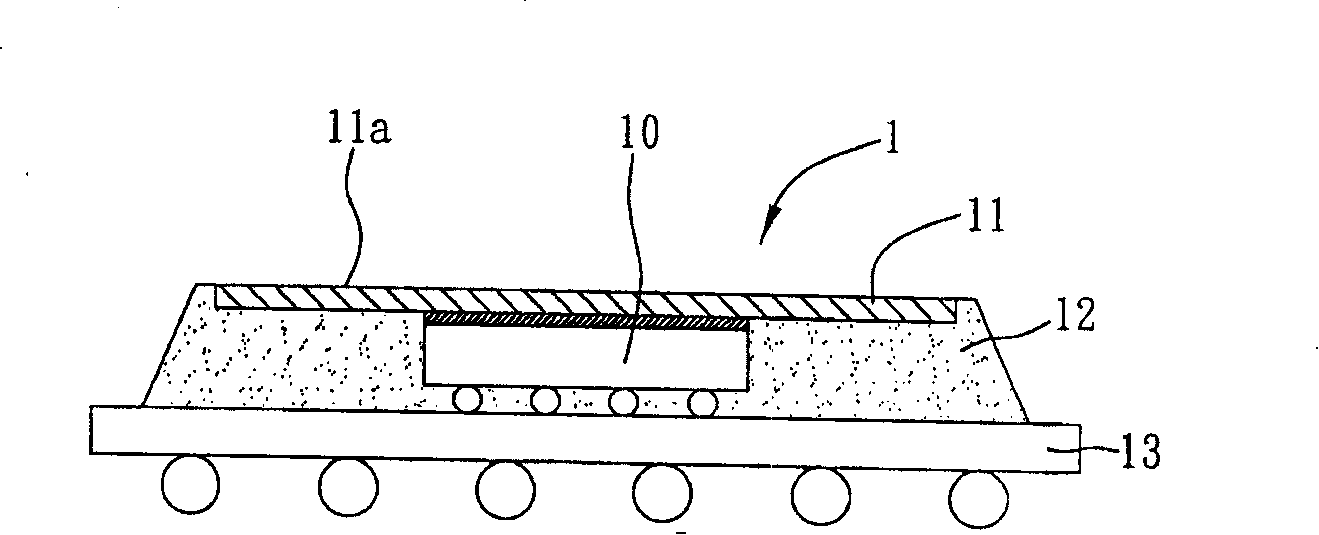
[0069] see Figure 4A to Figure 4F , is a schematic diagram of the first embodiment of the manufacturing method of the heat dissipation package of the present invention. The manufacturing method of the heat-dissipating package of the present invention can be used on a single chip carrier or batch-wise to process on a module chip with multiple chip carriers according to requirements.

[0070] Such as Figure 4A and Figure 4B shown, where the Figure 4B for corresponding to Figure 4A In the top view, firstly, the semiconductor chip is connected and electrically connected to the chip carrier 43 , and a heat dissipation structure 41 is connected to the semiconductor chip 40 .

[0071] The heat dissipation structure 41 includes a body 410 having a first surface 41a and a second surface 41b opposite to the first surface 41a, and a propping portion 411 protruding from the edge of the body 410 toward the first surface 41a, and on the first surface of the heat dissipation structu...

no. 2 example

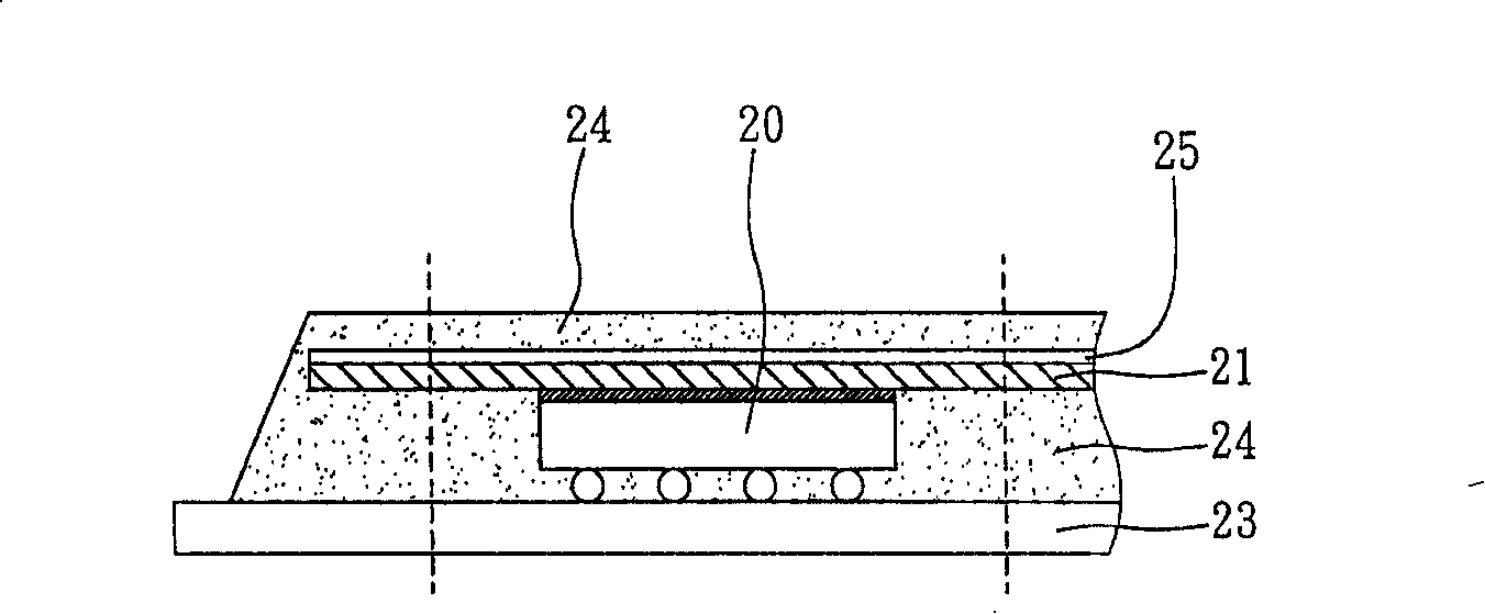
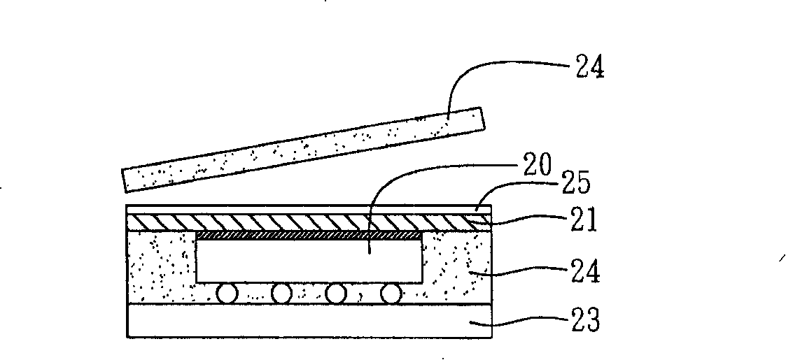
[0081] see Figure 6 , is a schematic diagram of the second embodiment of the manufacturing method of the heat dissipation package of the present invention. The manufacturing method of the heat-dissipating package of this embodiment is substantially the same as that of the previous embodiment, the main difference being that the material of the covering layer 65 formed on the heat-dissipating structure 61 is, for example, film, epoxy resin (epoxy), or wax (wax). The organic layer, its bonding force with the encapsulant 64 is greater than its bonding force with the heat dissipation structure 61, so during the removal operation, the covering layer 65 and the encapsulating compound 64 on the covering layer 65 will be removed at the same time, so as to The upper surface of the heat dissipating structure 61 is directly exposed, and then the heat of the semiconductor chip 60 is led out.

no. 3 example

[0083] see Figure 7 , is a schematic diagram of the third embodiment of the manufacturing method of the heat dissipation package of the present invention. As shown in the figure, the manufacturing method of the heat-dissipating package in this embodiment is substantially the same as that of the previous embodiments, the main difference is that a wire-bonded semiconductor chip 70 is placed on a chip carrier 73, and a plurality of bonding wires 700 is electrically connected to the chip carrier 73, and a spacer layer 78 such as a waste chip or a heat sink can be placed on the semiconductor chip 70, so that the heat dissipation structure 71 is connected to the semiconductor chip through the spacer layer 78 70 , preventing the heat dissipation structure 71 from touching the bonding wire 700 .

[0084] Therefore, the manufacturing method of the heat-dissipating package and the heat-dissipating structure used in the present invention are mainly to connect a heat-dissipating structu...


PUM


Abstract

The invention discloses a preparation method for a radiation package and a radiation structure used by the radiation package, wherein the method mainly comprises the steps of connecting a semi-conductor chip to and electrically on a chip carrier, and connecting a radiation structure to the semi-conductor chip; and the radiation structure is provided with a covering layer on the surface and convexly provided with a supporting part on the edge, wherein, the plan view size of the radiation structure is larger than that of the completed package, so the chip carrier connected with the semi-conductor chip and the radiation structure are arranged in a mould cavity of a packaging mould which is filled with packaging materials so as to form a package colloid covering the radiation structure and the semi-conductor chip, wherein, when the mould flowing velocity of the lower part of the radiation structure is higher than that of the upper part of the radiation structure for pushing and pressing the radiation structure upwards, the supporting part is pressed against the top surface of the mould cavity, thereby preventing the radiation structure from warping; then the package colloid on the covering layer can be cut and removed according to the preset plan view size of the package, thereby forming the radiation package.

Description

technical field [0001] The invention relates to a method for manufacturing a semiconductor package, in particular to a method for manufacturing a heat dissipation package and the applied heat dissipation structure. Background technique [0002] With the demand for thinner, lighter and smaller electronic products, semiconductor packages integrating high-density electronic components and semiconductor chips of electronic circuits have gradually become the mainstream of packaging products. However, since the semiconductor package generates high heat during operation, if the heat of the semiconductor chip is not quickly released in real time, the accumulated heat will seriously affect the electrical function and product stability of the semiconductor chip. On the other hand, in order to prevent the internal circuit of the package from being polluted by external water and dust, the surface of the semiconductor chip must be covered with an encapsulant to insulate it. However, the ...

Claims


Application Information

Patent Timeline
Patent Type & Authority Applications(China)
IPC IPC(8): H01L21/50H01L21/56H01L23/367
CPCH01L2224/16225H01L2224/73253
Inventor 洪敏顺蔡和易黄建屏廖俊明萧承旭
Owner SILICONWARE PRECISION IND CO LTD
Why Eureka
Try Eureka