
Reference circuit for restraining misadjusted CMOS energy gap

An energy gap reference and circuit technology, applied in the direction of adjusting electrical variables, control/regulating systems, instruments, etc., can solve the problems of mismatching and misalignment of op amp input stage tubes without substantial improvement, so as to overcome output misalignment and overcome input misalignment. effect of dissonance

Inactive Publication Date: 2008-07-23
WUXI SI POWER MICRO ELECTRONICS
View PDF0 Cites 28 Cited by
  • Summary
  • Abstract
  • Description
  • Claims
  • Application Information

AI Technical Summary

Problems solved by technology

For example, a cascode op amp with a two-stage differential structure is used, but this method only improves the gain of the op amp to a certain extent, and can only improve the offset caused by the limited gain of the op amp, and the mismatch of the input stage tubes of the op amp dissonance without substantial improvement

Method used


Image

  • Reference circuit for restraining misadjusted CMOS energy gap
  • Reference circuit for restraining misadjusted CMOS energy gap
  • Reference circuit for restraining misadjusted CMOS energy gap

Examples


Embodiment Construction

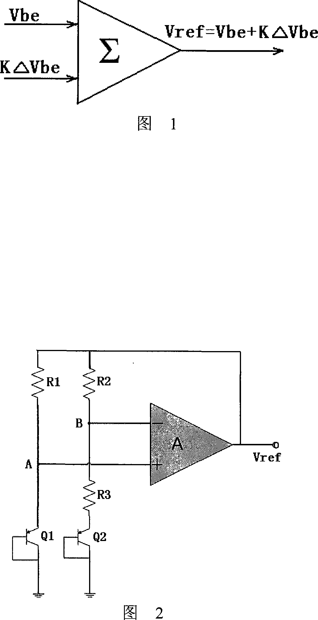
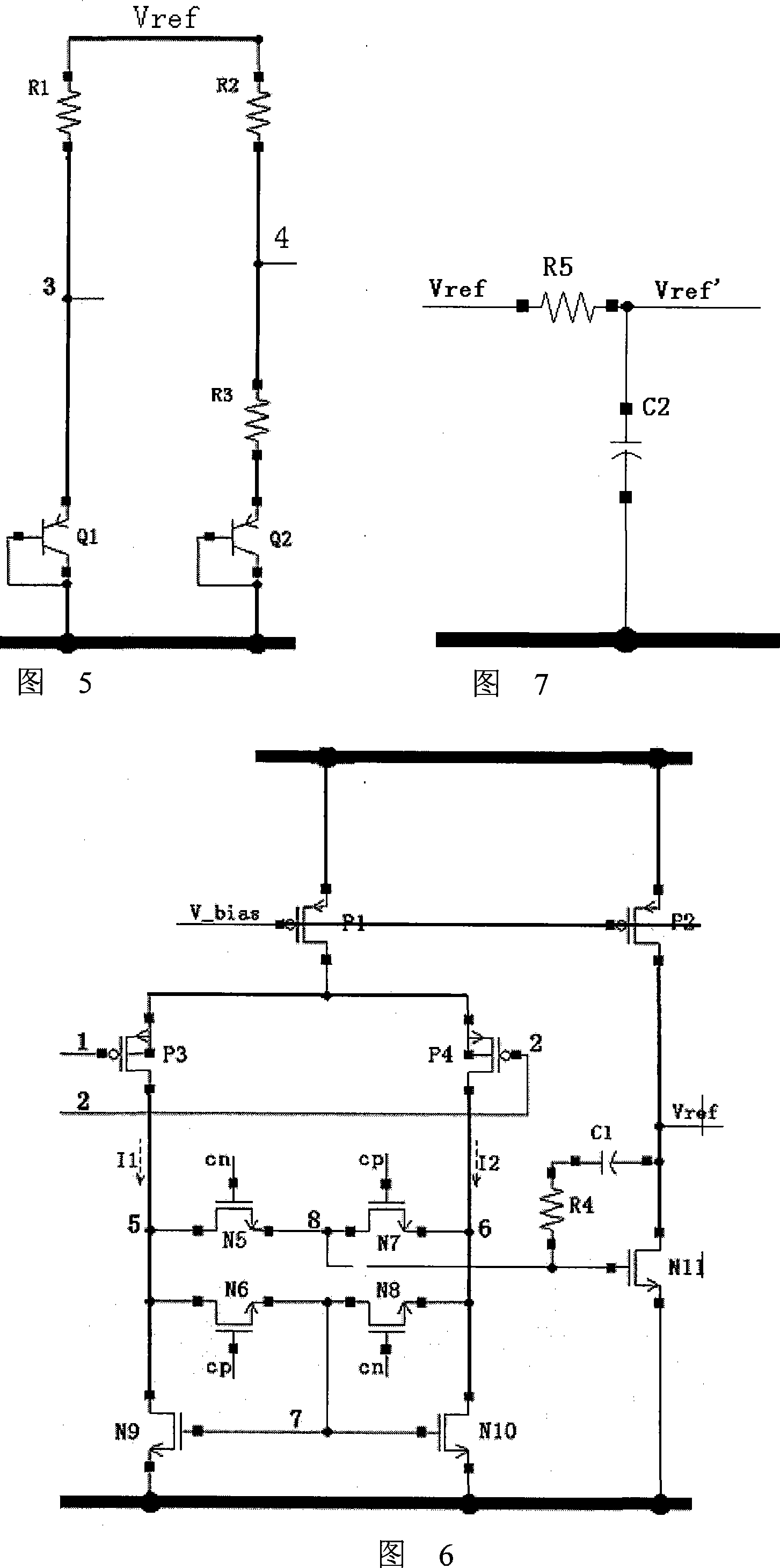
[0051] As shown in the figure: the CMOS bandgap reference circuit for suppressing misadjustment includes a bias circuit, a start-up circuit, a voltage addition circuit, an operational amplifier, and a filter circuit; it is characterized in that the start-up circuit is connected with the bias circuit to provide Start-up current; the bias circuit is connected to the current source of the operational amplifier to provide bias for the operational amplifier; the two output terminals of the voltage addition circuit are connected to the two input terminals of the operational amplifier through switch tubes N1~N4, wherein the gates of N2 and N3 Connect the clock signal cp, the gates of N1 and N4 are connected to the clock inversion signal cn; the two input terminals of the voltage addition circuit are connected to the output terminal of the operational amplifier; the output terminal of the operational amplifier is connected to the input of the filter circuit; the operational amplifier ha...


PUM


Abstract

The invention provides a CMOS energy gap reference circuit which can reduce disturbance. The inventive circuit comprises an input differential couple composed of PMOS tubes, a current mirror composed of NMOS tubes, a frequency compensation network composed of a capacitor C1 and a resistance R4, a filter network composed of a capacitor C2 and a resistance R5, a start circuit composed of a PMOS tube and a capacitor C3, a current source I1 for providing current to the differential couple, an addition circuit composed of resistance and transistor, and an input conversion circuit for switching and controlling the input. The input conversion circuit comprises a NMOS tube connected with the addition circuit and the differential input couple and a NMOS tube connected with the differential input grade and the common-emitter amplification grade. Since the input conversion circuit can convert the differential input couple continuously, the invention can reduce the reference error caused by disturbance.

Description

technical field [0001] The invention relates to a control circuit, in particular to a CMOS energy gap reference circuit for suppressing imbalance. Background technique [0002] The reference voltage source is widely used in various analog integrated circuits, digital-analog mixed-signal integrated circuits and system integrated chips (SOC). A basic element in . Its temperature stability and anti-noise ability are key factors affecting the conversion accuracy of A / D and D / A, and even affect the accuracy and performance of the entire system. With the development of the integrated circuit industry, SOC will become the mainstream of integrated circuit design in the future, and digital CMOS technology occupies an absolute dominant position in VLSI manufacturing. Therefore, it is of great significance to design a high-precision bandgap reference voltage source compatible with standard digital CMOS technology. [0003] In the past, people often used reverse breakdown zener diode...

Claims


Application Information

Patent Timeline
IPC IPC(8): G05F3/24
Inventor 丁国华冯开勇
Owner WUXI SI POWER MICRO ELECTRONICS
Learn More