
Apparatus and method for implementing high-precision buried resistance

A high-precision, wide-ranging technology, which is applied to the assembly of printed circuits with electrical components and the manufacture of multi-layer circuits, can solve the problems of poor precision of lateral etching size forming, complex process control, and influence on the accuracy of buried resistance. Effect of Improving Resistance Accuracy

Active Publication Date: 2008-07-23
HUAWEI DEVICE CO LTD
View PDF0 Cites 8 Cited by
  • Summary
  • Abstract
  • Description
  • Claims
  • Application Information

AI Technical Summary

Problems solved by technology

[0009]First, in the existing buried resistance processing flow, whether it is the forming dimension of the length direction of the etching buried resistance or the forming dimension of the etching buried resistance width direction, it is necessary to etch away The thickness of the copper foil layer is relatively large. When the copper foil layer is etched, it will produce a trapezoidal effect, which will directly lead to poor accuracy of the lateral etching size and affect the resistance accuracy of the final formed buried resistor.
[0010]Second, in the existing buried resistance processing flow, the thickness of the copper foil layer needs to be strictly controlled, but different process parameters are required for etching copper foil layers of different thicknesses. Will lead to more complex process control

Method used


Image

  • Apparatus and method for implementing high-precision buried resistance
  • Apparatus and method for implementing high-precision buried resistance
  • Apparatus and method for implementing high-precision buried resistance

Examples


Embodiment Construction

[0032] In order to make the object, technical solution and advantages of the present invention clearer, the implementation manner of the present invention will be further described in detail below in conjunction with the accompanying drawings.

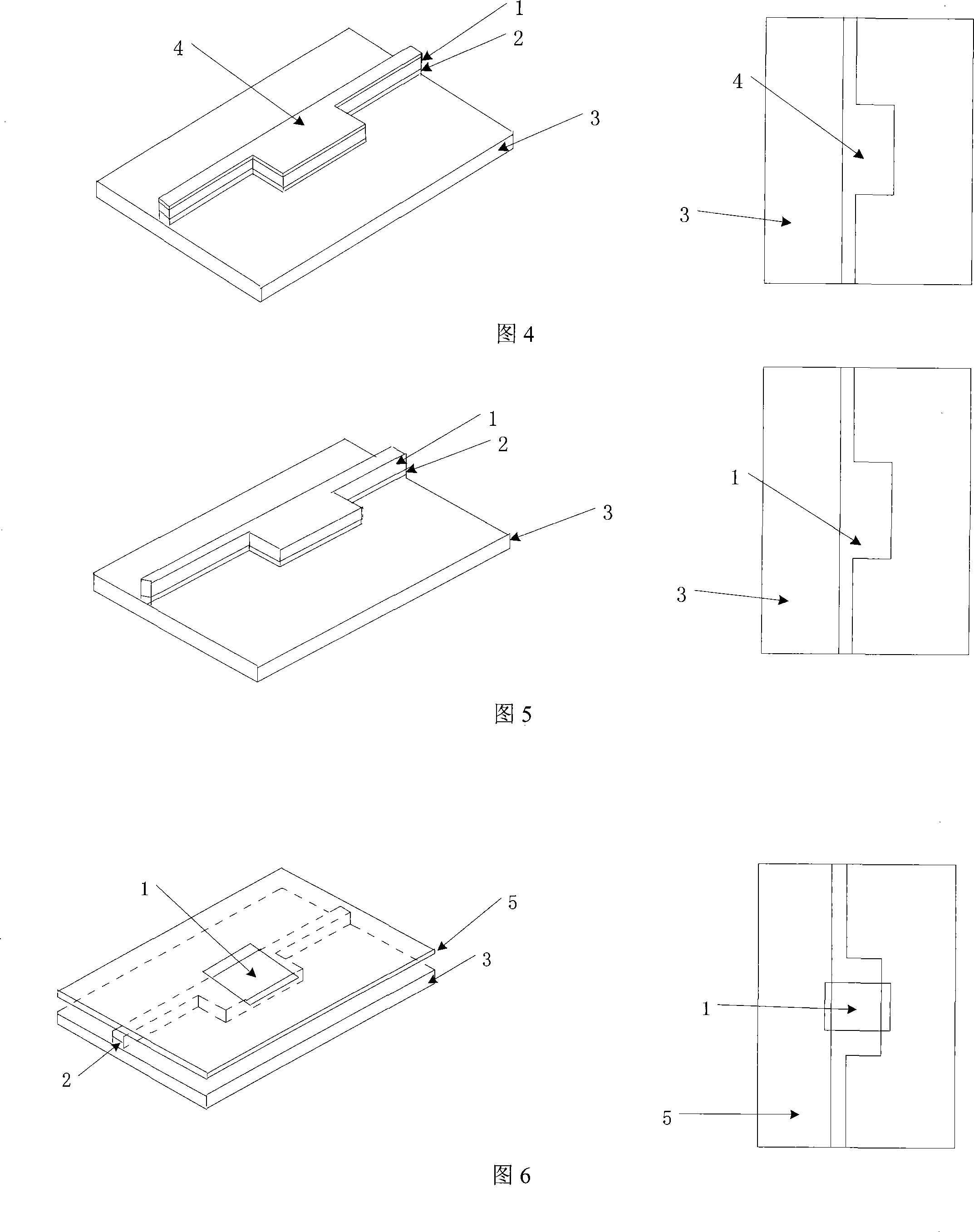
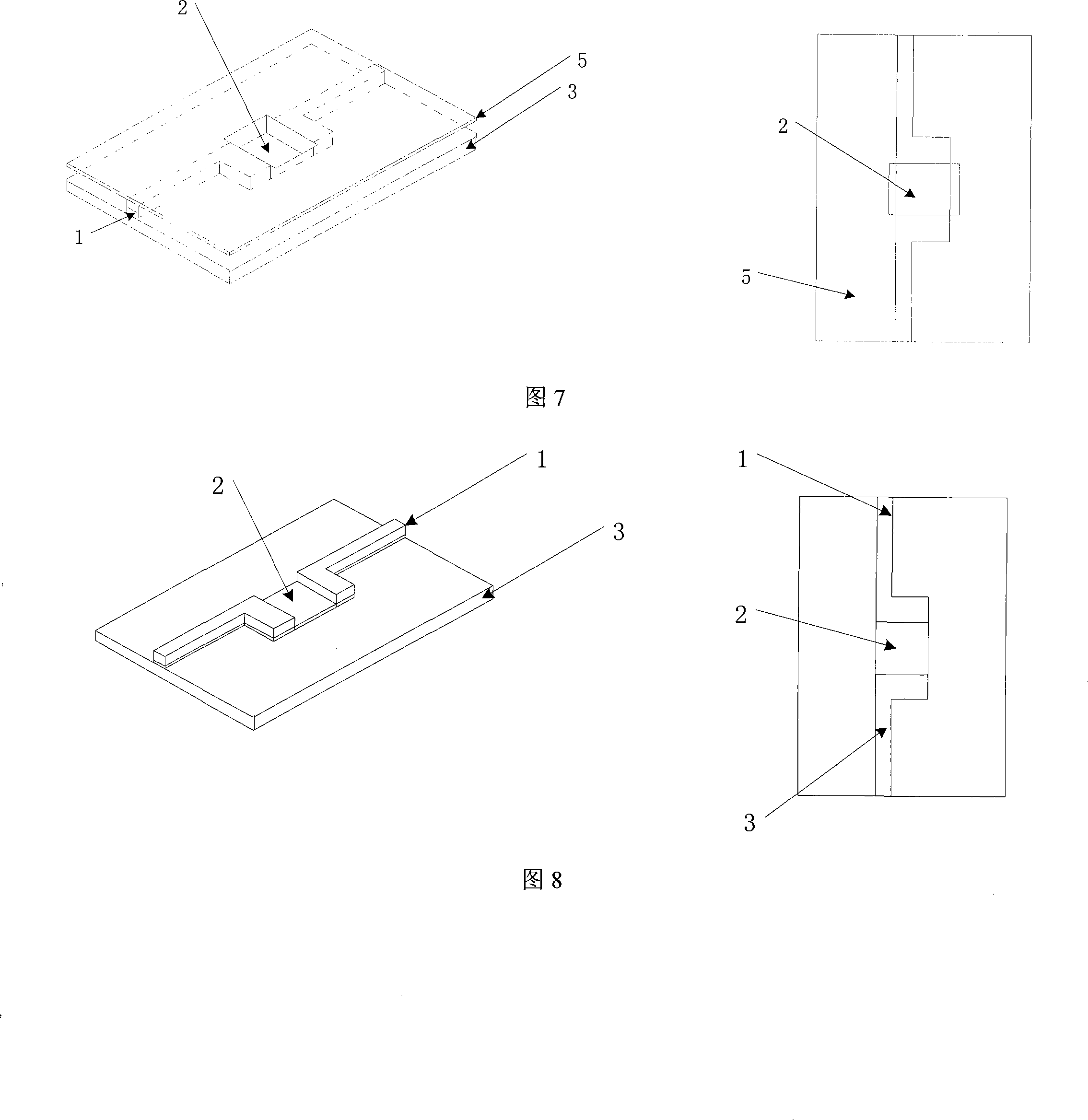
[0033] The embodiment of the present invention provides a method for realizing high-precision buried resistance. The method obtains the shape dimension and length direction of the buried resistance by etching the copper foil layer other than the interconnection lines of the preset buried resistance pattern and the non-buried resistance area. Interconnection lines in the non-buried resistance area; then measure the forming dimension in the length direction of the buried resistance, correct the forming dimension in the width direction of the buried resistance according to the calculation formula of the resistance value of the buried resistance, and etch according to the corrected forming dimension in the width direction of the buried resis...


PUM


Abstract

The invention discloses a method for realizing embedding resistance with high accuracy and a device, which belongs to the field of electronic equipment. The method comprises: etching prearranged embedded resistance pattern connecting terminals and a conducting layer outside interconnecting circuits in a non embedded resistance zone, obtaining molded dimension on the embedding resistance length direction and the interconnecting circuits in the non embedded resistance zone, measuring the molded dimension on the embedding resistance length direction, calculating correctional molded dimension on the embedding resistance length direction, and etching a resistance layer to obtain molded embedded resistance according to the correctional molded dimension on the embedding resistance length direction. The technical scheme of the invention firstly etches the molded dimension on the embedding resistance length direction and the interconnecting circuits in the non embedded resistance zone and then errors which are produced by etching the molded dimension on the embedding resistance length direction are corrected through etching the molded dimension on the embedding resistance length direction, which is beneficial for increasing the resistance precision of the embedding resistance which is finally molded and enables an embedding resistance producing technique to be controlled easier.

Description

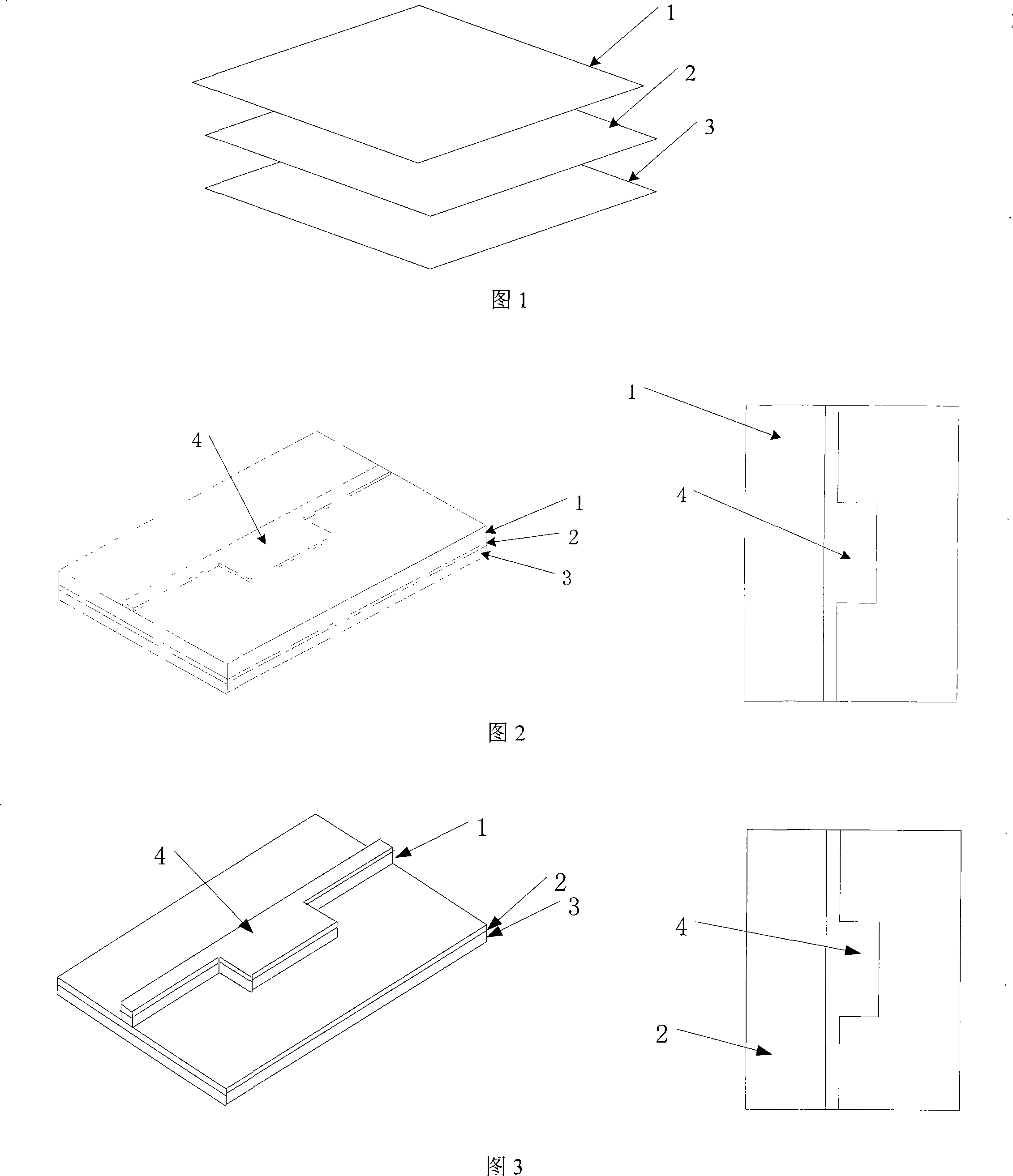
technical field [0001] The invention relates to the field of electronic equipment, in particular to a method and device for realizing high-precision buried resistance. Background technique [0002] The planar embedded resistance technology adopts the conventional printed board subtractive production process to integrate the resistors into the multilayer printed board. Plane buried resistance technology has become the most mature technology in circuit design because of its high performance, low cost and long-term stability. The application of planar buried resistance technology has the following advantages: good electrical performance, high density of buried resistance, better reliability of buried resistance and low cost. As shown in Figure 1, the buried resistance structure is composed of three layers of materials: copper foil layer 1 (can also be other conductor layers), nickel-phosphorus alloy thin film 2 (also can be other resistance layers) and insulating substrate 3 ....

Claims


Application Information

Patent Timeline
IPC IPC(8): H05K3/30H05K3/46
Inventor 王洪利
Owner HUAWEI DEVICE CO LTD
Learn More