High light transmittance ratio glass display protection panel and LCD device using same
A liquid crystal display, high light transmittance technology, applied in shielding, instruments, optics, etc., can solve the problems of reducing the surface reflectivity of protective screen materials, no fundamental changes, and difficult control of film thickness, etc., to achieve low cost, reduce light High reflectivity and high production efficiency
- Summary
- Abstract
- Description
- Claims
- Application Information
AI Technical Summary
Problems solved by technology
Method used
Image
Examples
Embodiment 1
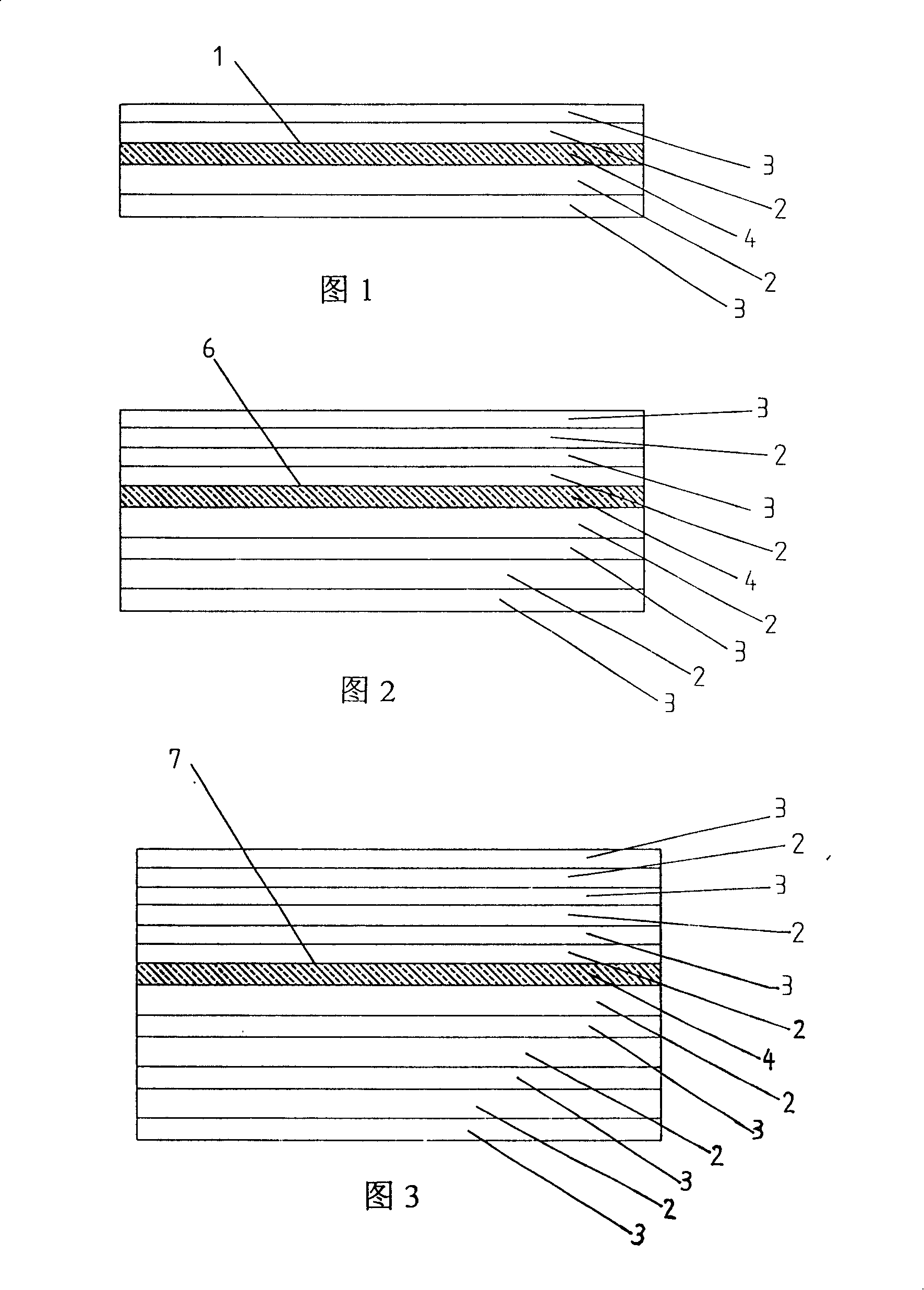
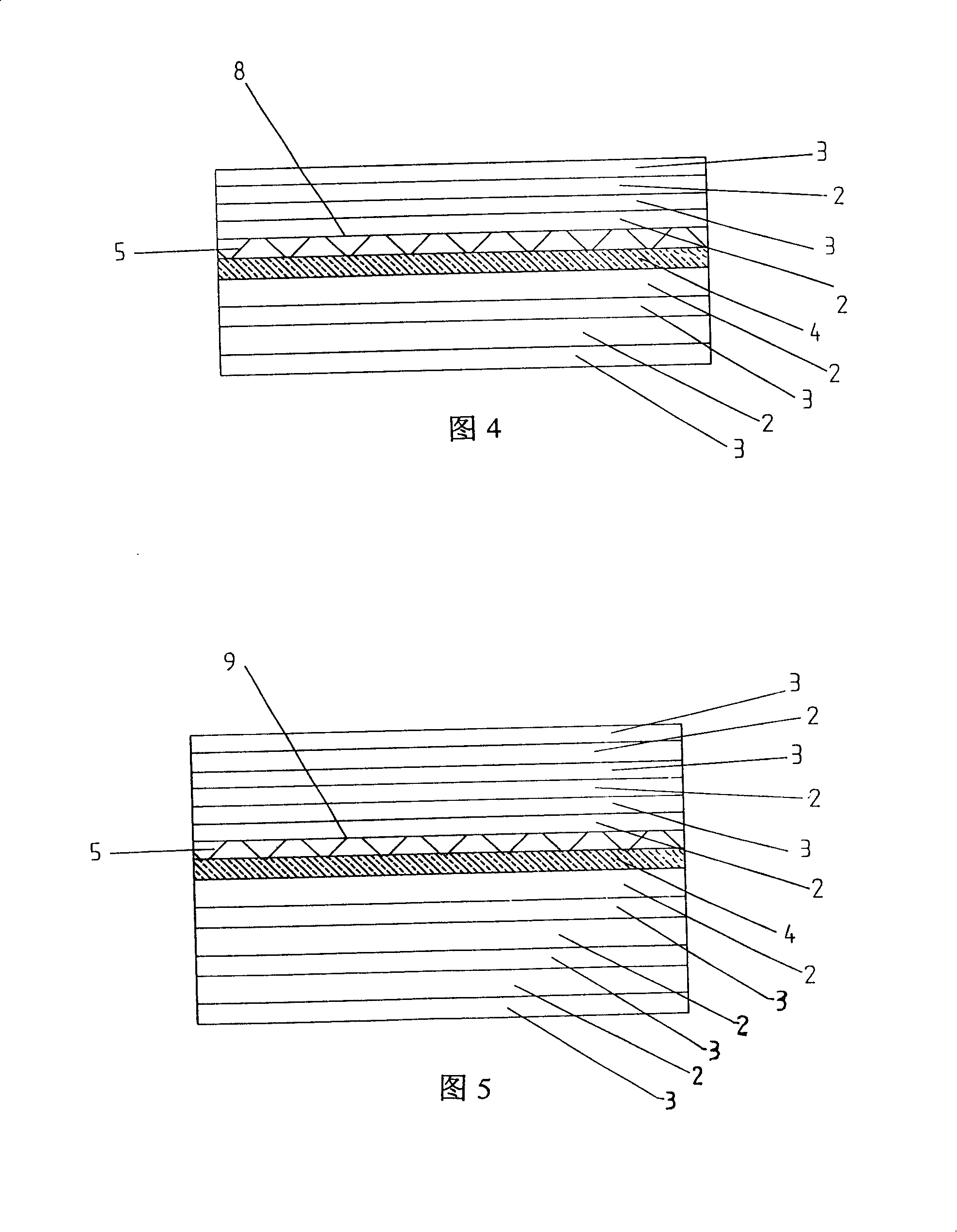
[0024] Fig. 1 has provided present embodiment 1 figure. Referring to Fig. 1, the display protection screen 1 of high transmittance glass is made of a transparent glass substrate 4 and two layers of anti-reflection and anti-reflection TiO deposited sequentially on both sides of the substrate 4 by vacuum magnetron sputtering. 2 Coating 2 and SiO 2 film layer 3, and the formation structure is SiO 2 / TiO 2 / Glass substrate / TiO 2 / SiO 2 Display protection screen 1 of high transmittance glass. Two layers of anti-reflection and anti-reflection coatings are coated on both sides of the substrate 4, the light transmittance is greater than 94%, the double-sided superimposed reflectance is less than 2%, and the optimized thickness of the coating is: TiO 2 10~16nm, SiO 2 It is 90~120nm.
Embodiment 2
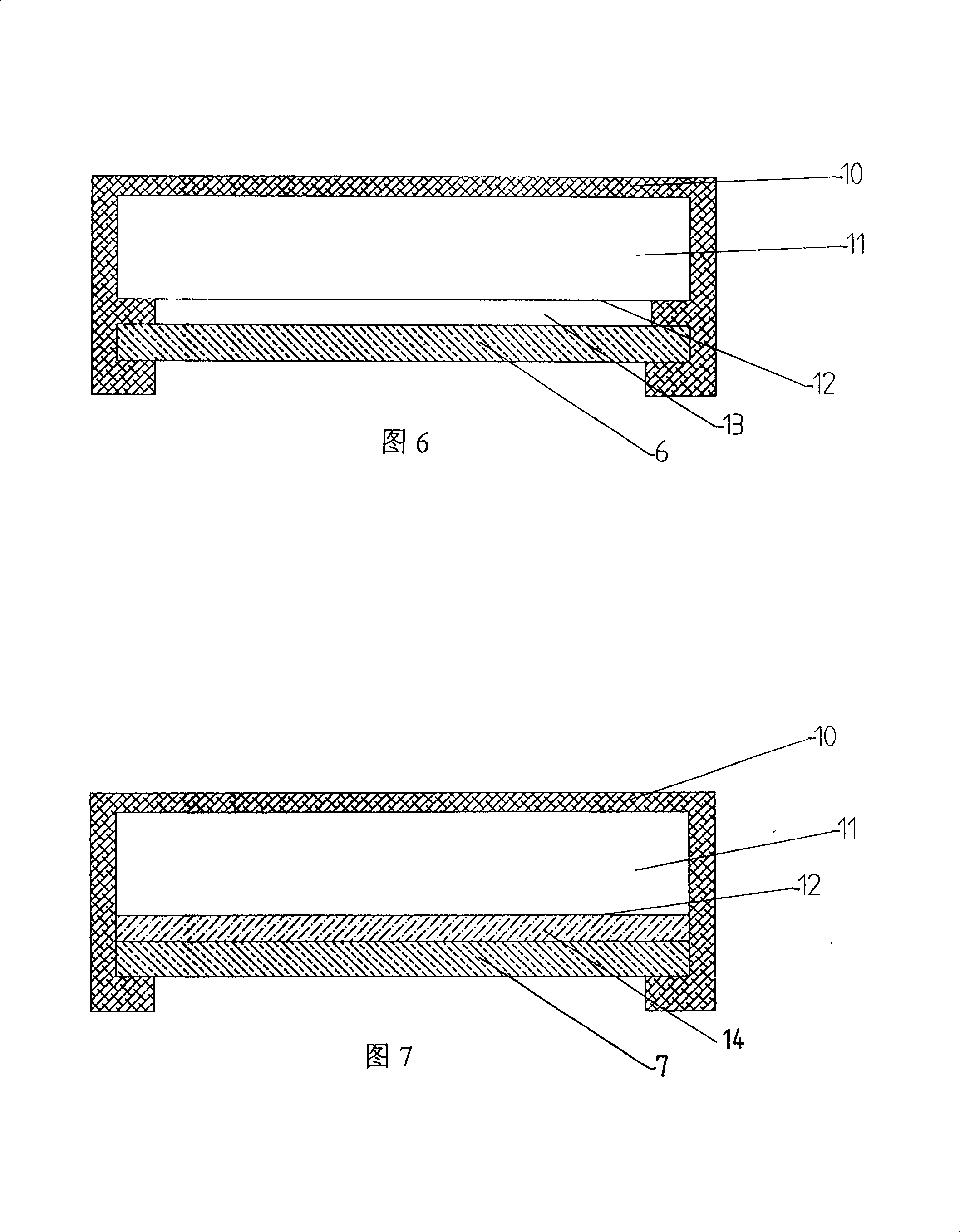
[0026] Figure 2 shows the structure diagram of Embodiment 2. This embodiment 2 is basically the same as embodiment 1, the difference is that each of the two sides of the substrate 4 is coated with four layers of anti-reflection and anti-reflection coating layers, and the formation structure is SiO 2 / TiO 2 / SiO 2 / TiO 2 / Glass substrate / TiO 2 / SiO 2 / TiO 2 / SiO 2 Display protection screen 6 made of high-transmittance glass, the light transmittance on both sides is greater than 97%, and the reflectivity on both sides is less than 1.5%. The optimized thickness of the coating is as follows: SiO 2 100~115nm / TiO 2 30~36nm / SiO 2 36~45nm / TiO 2 8~12nm / glass substrate / TiO 2 8~12nm / SiO 2 36~45nm / TiO 2 30~36nm / SiO 2 It is 100~115nm.
Embodiment 3
[0028] Fig. 3 has provided the figure of present embodiment 3, and this implementation is basically the same as embodiment 2, and difference is that the two sides of substrate 4 are coated with six layers of anti-reflection and anti-reflection coating layers respectively, and the formation structure is SiO 2 / TiO 2 / SiO 2 / TiO 2 / SiO 2 / TiO 2 / Glass substrate / TiO 2 / SiO 2 / TiO 2 / SiO 2 / TiO 2 / SiO 2 High light transmittance glass display protection screen 7, the light transmittance is greater than 98.5%, the double-sided superimposed reflectivity is less than 1%, and the optimized thickness of the coating is as follows: SiO 2 100~130nm / TiO 2 12~18nm / SiO 2 40~60nm / TiO 2 8~12nm / SiO 2 30~40nm / TiO 2 1~3nm / glass substrate / TiO 2 1~3nm / SiO 2 30~40nm / TiO 2 8~12nm / SiO 2 40~60nm / TiO 2 12~18nm / SiO 2 100-130nm.
PUM
| Property | Measurement | Unit |
|---|---|---|
| Thickness | aaaaa | aaaaa |
| Surface resistance | aaaaa | aaaaa |
Abstract
Description
Claims
Application Information


