Analog PCB intelligent test system based on neural network

A test system and neural network technology, which is applied in the field of neural network-based analog PCB intelligent test system, can solve the problems of initial weight vector sensitivity, etc., and achieve the effects of facilitating engineering implementation, improving fault diagnosis resolution, and building flexibility

Inactive Publication Date: 2008-08-20
HUNAN UNIV
View PDF0 Cites 33 Cited by
  • Summary
  • Abstract
  • Description
  • Claims
  • Application Information

AI Technical Summary

Problems solved by technology

However, the BP network uses a search algorithm that descends along the gradient, so it i

Method used


Image

  • Analog PCB intelligent test system based on neural network
  • Analog PCB intelligent test system based on neural network
  • Analog PCB intelligent test system based on neural network

Examples


Embodiment Construction

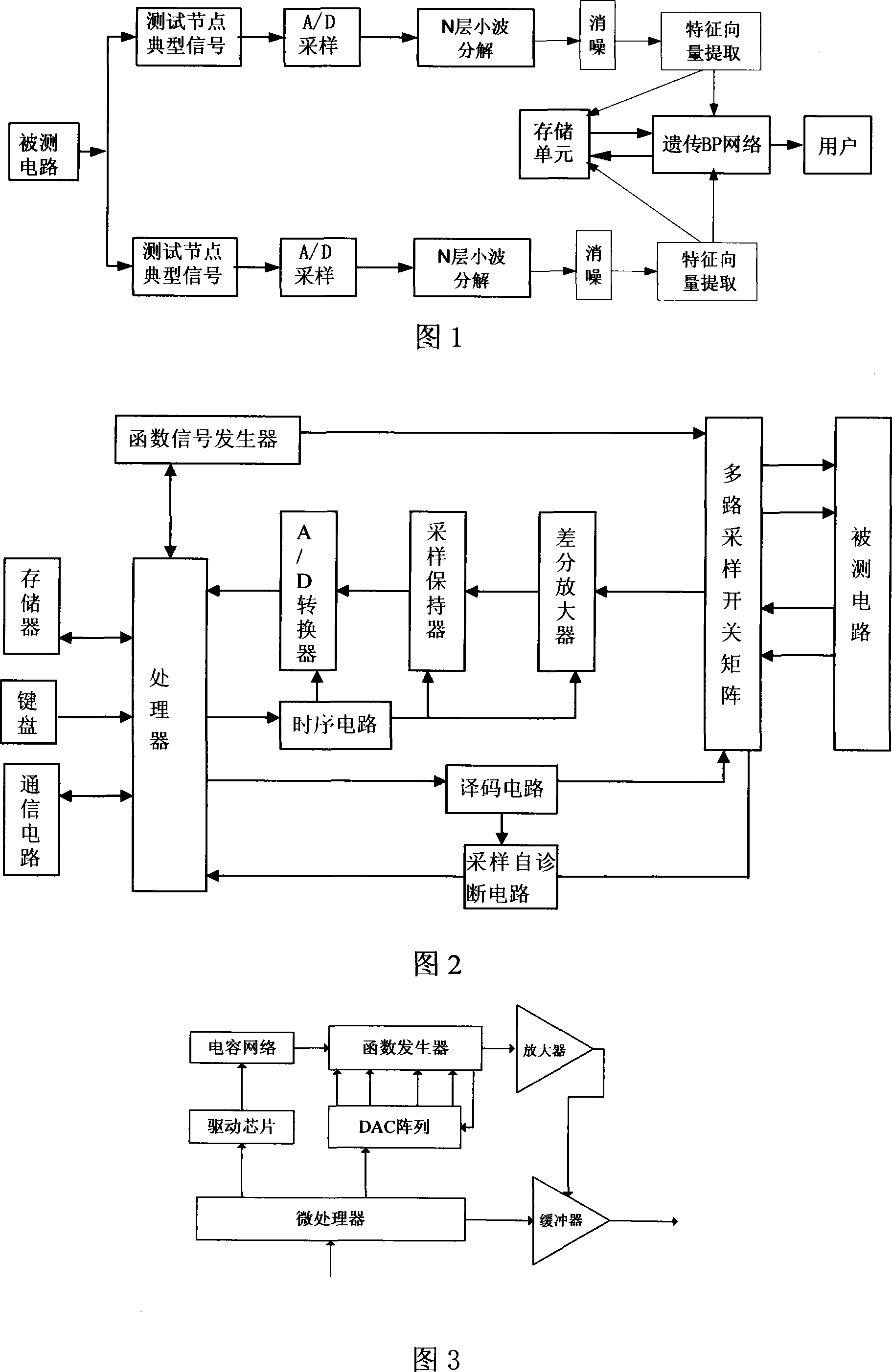
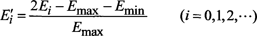
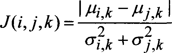
[0013] Referring to FIG. 1, the present invention includes a processor, a memory, a communication circuit, a function signal generator, a multi-channel sampling switch matrix, a sequential circuit, a decoding circuit, an A / D converter, a sample-and-hold, and a differential amplifier. The decoding Circuits, sequential circuits, A / D converters, sample holders, differential amplifiers, and multi-channel sampling switch matrix form a sampling circuit to complete the sampling of test signals. Communication with the host computer, the function signal generator output excitation signal under the control of the processor is sent to the excitation node of the circuit under test through the multi-channel sampling switch matrix.

[0014] The processor in the present invention can adopt TMS320C5416DSP chip, 4mbitflash, 256k*16bit SRAM, 2500gate CPLD and a JTAG socket produced by TI Company, and the socket can be used to perform experiments through the emulator and CCS download program; Th...


PUM


Abstract

The invention discloses a simulating PCB intelligent test system which is based on nerve network, which includes main control PC machine, processor, storage, communication circuit, function signal generator, multi-channel sampling switch matrix, sequential circuit, decoding circuit, A/D converter, sampling retainer, differential amplifier, function signal generator under the control of processor outputs stimulating signal to the stimulating node of the tested circuit, the responding signal of the tested circuit is transmited to the processor by multi-channel sampling circuit, then is transmitted to the main control PC machine by communication circuit, the main control PC machine treats the sampling signal with wavelet packet transform de-noising treatment, and with principal component analysis and normalization processing for obtaining fault feature vector; the fault feature vector is inputted into the trained BP nerve network, the output of the BP nerve network is fault type. The invention can position the PCB test fault to the component level effectively, and improve the scalability of system greatly with the simple and effective test method of CMOS switch array.

Description

technical field [0001] The invention relates to a simulated PCB test system, in particular to a simulated PCB intelligent test system based on a neural network. Background technique [0002] With the development of large-scale analog integrated circuits, the complexity and density of analog circuits continue to grow, and the failure of any component or device will affect the overall situation, so more stringent requirements are placed on the reliability of analog circuit operation; After the analog circuit fails, it is required to locate the fault in real time for maintenance, debugging and replacement. In essence, the analog circuit fault diagnosis is actually equivalent to a classification problem, which is to determine which fault class the circuit state belongs to according to the measurement data. The traditional classification and diagnosis methods require a lot of calculation, especially due to the influence of tolerance, the calculation is quite complicated and the ...

Claims


Application Information

Patent Timeline
IPC IPC(8): G01R31/316G06N3/06
Inventor 何怡刚祝文姬谢宏刘美容王玺庞伟区肖迎群谭阳红邓晓
Owner HUNAN UNIV
Why Eureka
Try Eureka