Semiconductor package structure and manufacturing method thereof

A technology of packaging structure and manufacturing method, applied in semiconductor/solid-state device manufacturing, semiconductor devices, semiconductor/solid-state device components, etc., can solve the problems of increasing power consumption, unable to ensure stable control of characteristic impedance, and increasing thermal resistance, etc. Effects of reducing parasitic impedance and inductance, improving reliability, and reducing thermal resistance

Active Publication Date: 2008-08-27
ADVANCED SEMICON ENG INC
View PDF0 Cites 2 Cited by
  • Summary
  • Abstract
  • Description
  • Claims
  • Application Information

AI Technical Summary

Problems solved by technology

However, the slender single-layer line cannot ensure the stable control of the characteristic impedance under the high-speed and high-frequency signal transmission, and even causes power supply noise and signal rebound in severe cases. This is its primary shortcoming.
[0004] Furthermore, with the increase in the number and density of components in a single integrated circuit (IC) chip, the power consumption is relatively increased, and the redistribution layer can redistribute the bonding pads to the chip through the thin and long lines. Perimeter, both sides or any side, but it also makes it difficult to dissipate heat, causing the temperature of the IC chip to rise, which in turn affects its characteristics and performance, resulting in a decrease in chip yield. This is another shortcoming
[0005] Therefore, the existing redistribution layer uses long and thin trace design to redistribute the positions of the pads of the signal input and output terminals, which will cause the disadvantages of excessively high parasitic resistance, insufficient voltage supply, and uncontrollable characteristic impedance.
Furthermore, the slender line design will also increase the thermal resistance and reduce the yield of the chip

Method used


Image

  • Semiconductor package structure and manufacturing method thereof
  • Semiconductor package structure and manufacturing method thereof
  • Semiconductor package structure and manufacturing method thereof

Examples


Embodiment Construction

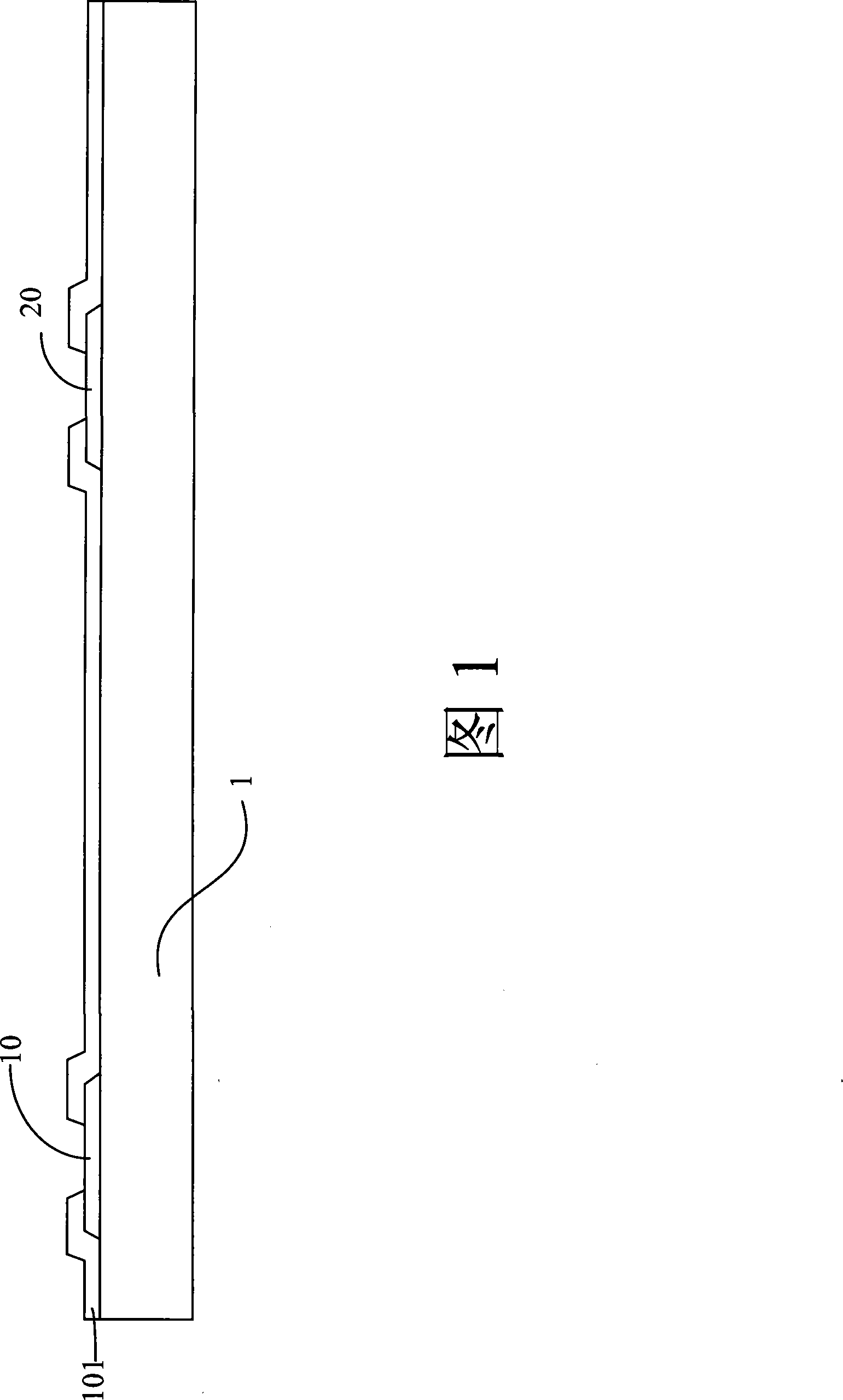
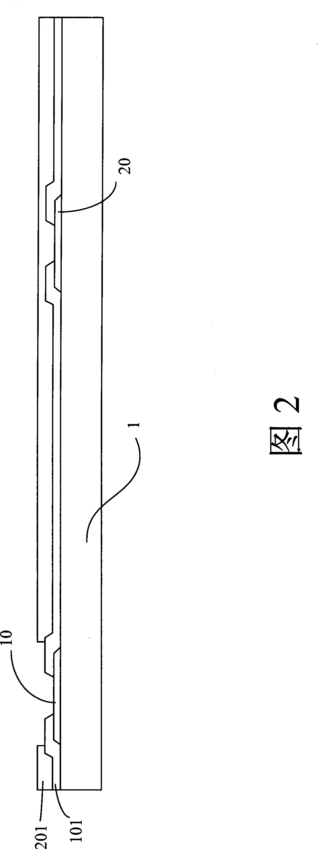
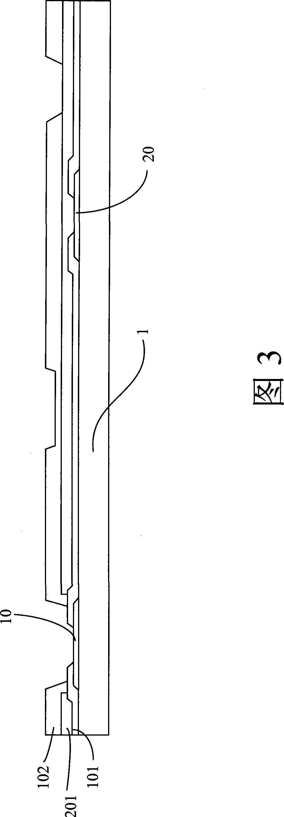
[0025] The semiconductor package structure of the present invention will be described below with reference to the drawings, and the semiconductor package structure of the present invention and its manufacturing method will be described in detail with reference to the structural schematic diagrams shown in FIGS. 1 to 6 . It should be noted here that "up" and "down" here refer to the directions shown in the relevant drawings, and are mainly tentative directional terms for the description herein, and are not used to limit the present invention.

[0026] FIG. 1 schematically shows the structure after the first protective layer is formed according to the manufacturing method of the semiconductor package structure of the present invention. As shown in FIG. 1 , firstly, a semiconductor substrate 1 is provided, such as a wafer, having a surface 100 with at least one first pad 10 and at least one second pad 20 thereon. Then a first protection layer 101 is formed to cover the surface 10...


PUM


Abstract

The invention discloses a semiconductor packaging structure, which comprises a semiconductor base material, a first passivation layer, a first metallic layer, a second passivation layer, a second metallic layer and a third metallic layer, wherein, the semiconductor base material is provided with a surface; at least one first welded gasket and at least one second welded gasket are arranged on the surface; the first passivation layer covers the surface of the semiconductor base material and exposes the first welded gasket and the second welded gasket; the first metallic layer is formed on the first passivation layer and electrically connected with the second welded gasket; the second passivation layer is formed on the first metallic layer and exposes the first welded gasket and a part of the first metallic layer; the second metallic layer is formed on the second passivation layer and electrically connected with the first welded gasket; the third metallic layer is formed on the second passivation layer and electrically connected with the first metallic layer.

Description

technical field [0001] The present invention relates to a semiconductor packaging structure and its manufacturing method, and in particular to a redistribution layer (Re-Distribution Layer; RDL) structure and its manufacturing method. Background technique [0002] With the development trend of electronic products towards light, thin, short, and small, correspondingly, the packaging type will also develop towards the design of higher density pins, and thus many new types of packaging methods will be produced. These new types The packaging methods include: (1) Ball grid array (BGA), which is connected to the circuit board by means of solder balls, replaces the traditional pins with solder balls, and arranges the solder balls in an array mode; (2) ) Inverted crystal package (Flip Chip) with the crystal face down and combined with the substrate through tin-lead bumps; (3) Quad Flat Package (QFP), etc. In addition to the above, the most advantageous packaging technology in the e...

Claims


Application Information

Patent Timeline
Patent Type & Authority Applications(China)
IPC IPC(8): H01L23/485H01L21/60
CPCH01L24/11H01L2224/11H01L2924/14H01L2924/00H01L2924/00012
Inventor 郑宏祥黄志亿
Owner ADVANCED SEMICON ENG INC
Why Eureka
Try Eureka