Method for making printed circuit board and etched half-finished circuit board

A technology for printed circuit boards and manufacturing methods, which is applied in the direction of printed circuits, printed circuit manufacturing, printed circuit components, etc., and can solve problems such as damage to thin core boards, low pass rate, and product scrapping

Inactive Publication Date: 2008-09-10
SHENZHEN FASTPRINT CIRCUIT TECH
View PDF0 Cites 4 Cited by
  • Summary
  • Abstract
  • Description
  • Claims
  • Application Information

AI Technical Summary

Problems solved by technology

[0003] When the thickness of the dielectric layer of the core board is less than 0.13mm, it becomes very difficult to develop, etch and remove the film in the process of making the inner layer pattern of the circuit board, especially in the current processing technology, the circuit pattern is placed on the circuit board The base copper in the other areas is corroded, ma...

Method used


Image

  • Method for making printed circuit board and etched half-finished circuit board
  • Method for making printed circuit board and etched half-finished circuit board
  • Method for making printed circuit board and etched half-finished circuit board

Examples


Embodiment Construction

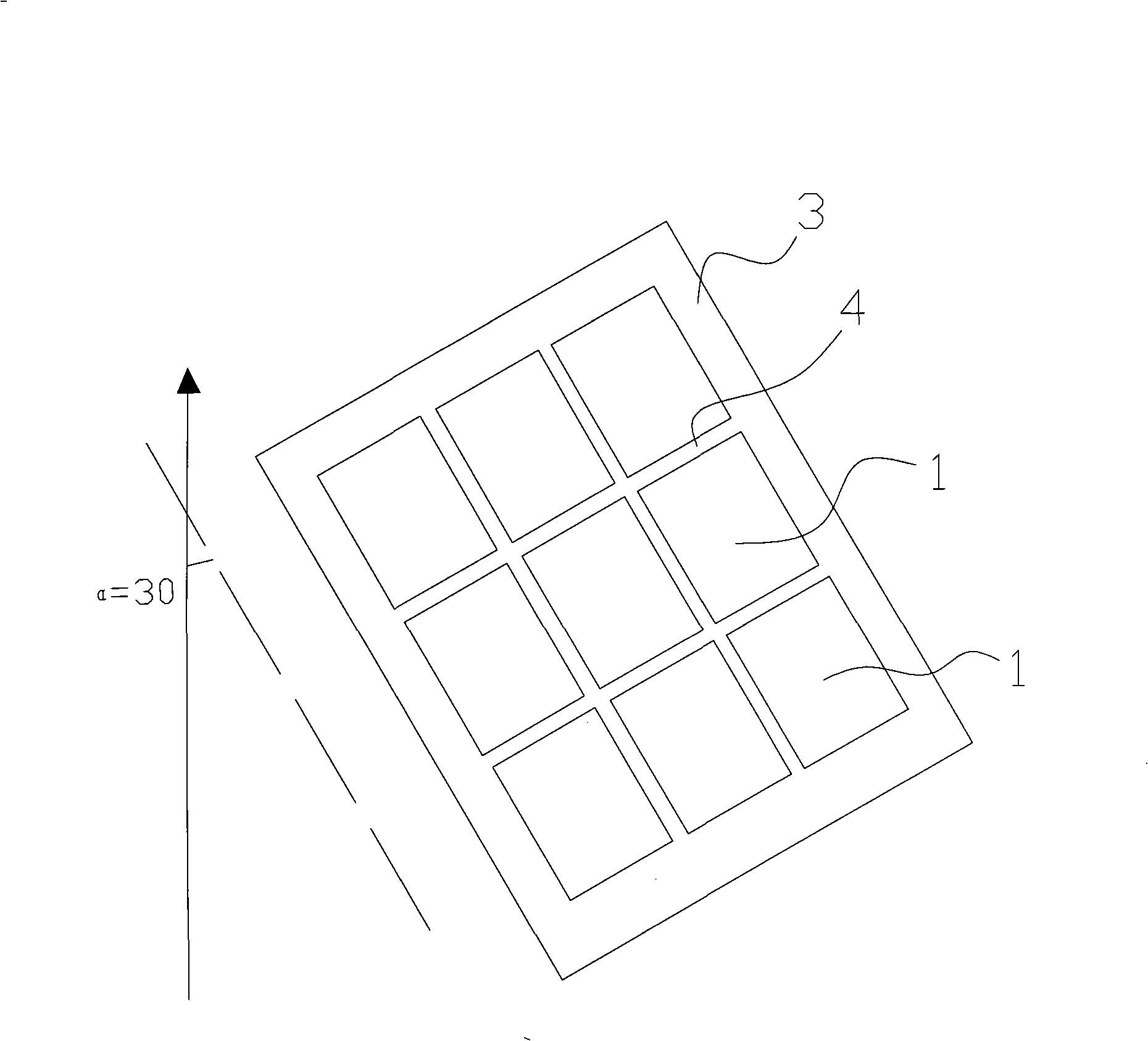
[0029] Such as figure 2 , image 3 As shown, a method for manufacturing a printed circuit board at least includes the following steps:
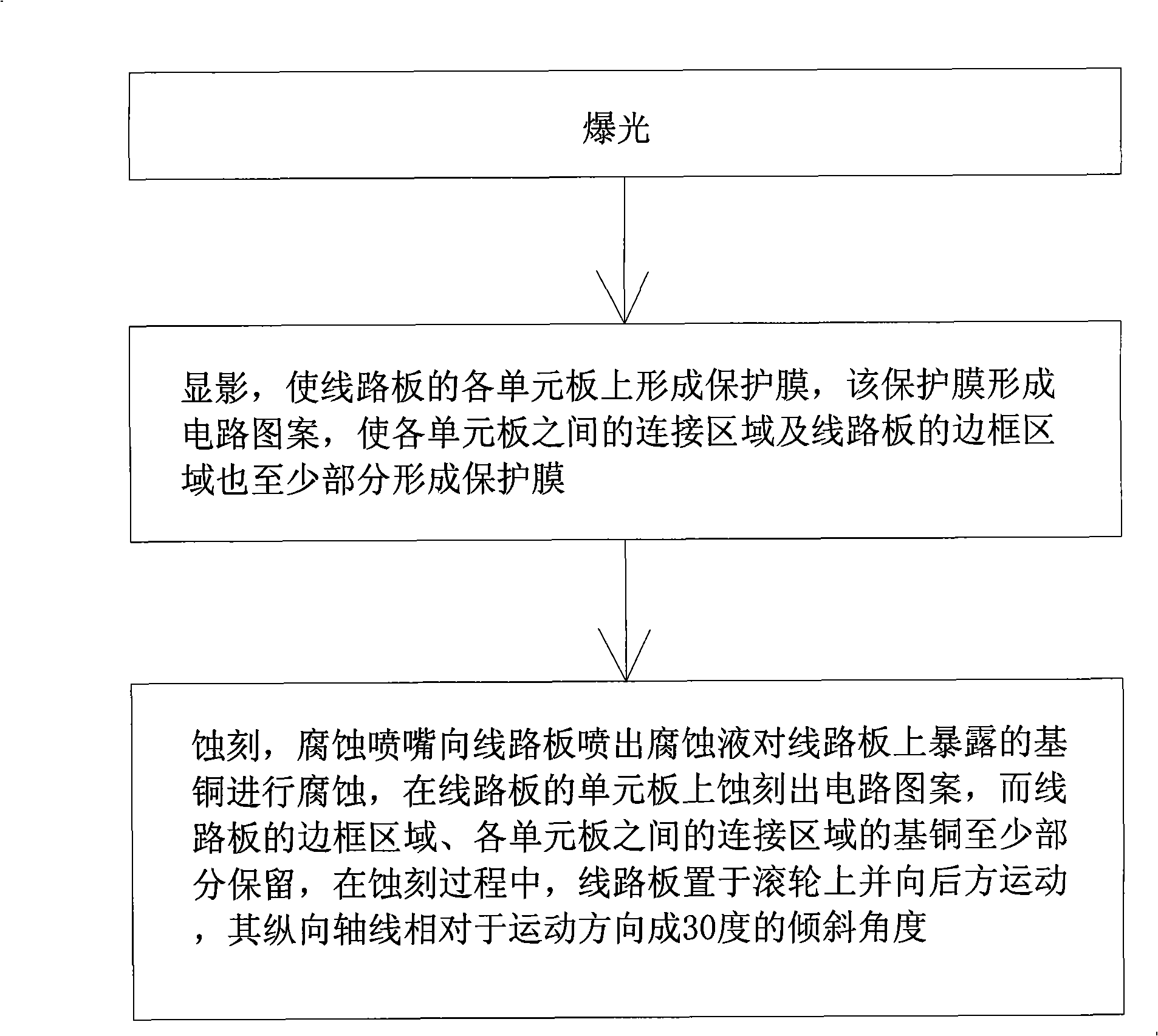
[0030] a. exposure;

[0031] B. develop, make each unit board 1 of circuit board form protective film, this protective film forms circuit pattern, make the connection area 4 between each unit board 1 and the frame area 3 of circuit board also at least partially form protective film;

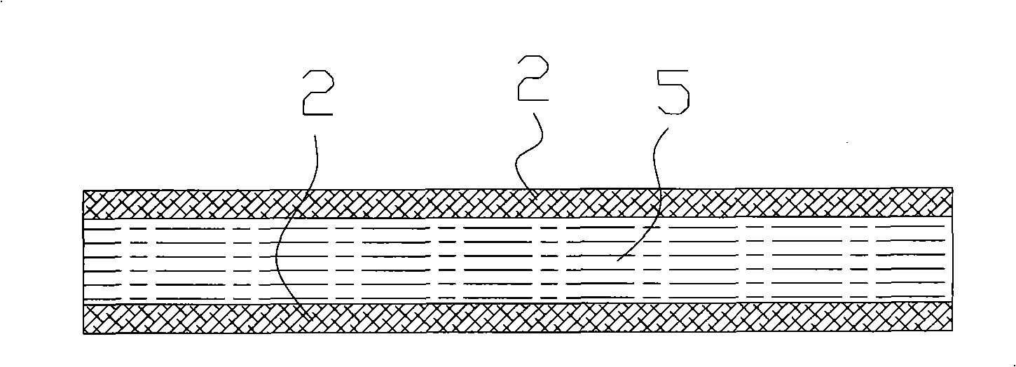
[0032] c. Etching, the corrosion nozzle sprays corrosive liquid to the circuit board to corrode the exposed base copper on the circuit board, and etches a circuit pattern (not shown in the figure) on the unit board 1 of the circuit board, while the frame area of ​​the circuit board 3. The base copper part of the connection area 4 between the unit boards 1 is reserved. During the etching process, the circuit board is placed on the roller and moves backward, and its longitudinal axis forms an inclination angle of 30 degrees relative to the direction of motion. ...


PUM

PropertyMeasurementUnit
Slopeaaaaaaaaaa

Abstract

The invention discloses a method for manufacturing a printed wiring board and an etched semi-finished wiring board. The method at least comprises the steps as follows: a. exposing; b. developing: a protective film is caused to form on each unit plate of the wiring board, and the protective film forms a circuit pattern, protective films are also caused to form on at least some parts of connection areas between the unit plates and frame areas of the wiring board; c. etching: an erosion nozzle sprays erosive liquid to the wiring board to erode an exposed base copper on the wiring board, and circuit patterns are etched on the unit plates of the wiring board while at least some part of the base copper in the frame areas of the wiring board and the connection areas between the unit plates is reserved; by adopting the method, the base copper is still reserved on the surfaces of two sides of either the connection areas or the frame areas of the etched semi-finished wiring board so as to form an reinforced copper block. In the etching and follow-up procedures of the wiring board, the strength and rigidity of the wiring board are improved, with low breakdown rate and high product qualification rate.

Description

technical field [0001] The invention relates to a manufacturing method of a printed circuit board and an etched semi-finished circuit board. Background technique [0002] At present, all kinds of electronic products are constantly developing in the direction of low power consumption, multi-function, and high reliability, but the size of the products is constantly tending to be miniaturized, even miniaturized. During the processing of various electronic products, often Printed circuit boards are used, and circuit boards play a very critical role as the carrier of electronic components. In order to meet the requirements of high density, number of layers and thinner thickness of the circuit board, a thinner inner core board is used in the production process. The thickness of the thin core board is much lower than the conventional lower limit of 0.13mm, as thin as 0.05-0.10 mm, the structure of the thin core board before processing is as figure 1 As shown, it includes the diel...

Claims


Application Information

Patent Timeline
IPC IPC(8): H05K3/02H05K1/02
Inventor 乔书晓
Owner SHENZHEN FASTPRINT CIRCUIT TECH
Why Eureka
Try Eureka