Semiconductor device

A semiconductor and wire technology, applied in the field of semiconductor devices, can solve problems such as poor work, deterioration of work quality, and increase in chip size, and achieve the effect of reducing chip size, reducing impact, and preventing chip size increase.

Inactive Publication Date: 2008-09-10
PANASONIC SEMICON SOLUTIONS CO LTD
View PDF1 Cites 1 Cited by
  • Summary
  • Abstract
  • Description
  • Claims
  • Application Information

AI Technical Summary

Problems solved by technology

[0007] However, in such a semiconductor device, in a semiconductor device using a staggered pad configuration, it is difficult to avoid contact between the pads and the connecting wires between the semiconductor elements, and therefore, electrical short circuits, Due to the malfunction caused by the above situation, etc., the deterioration of the quality of the work is caused, and when the distance between the pads or the leads is made large to prevent the electrical short circuit caused by the contact between the above-mentioned connecting wires, there is a possibility that the chip size will increase. big problem

Method used


Image

  • Semiconductor device
  • Semiconductor device
  • Semiconductor device

Examples


Embodiment approach 1

[0190] Hereinafter, the semiconductor device 300 (semiconductor device 1 ) according to Embodiment 1 of the present invention will be described with reference to the drawings.

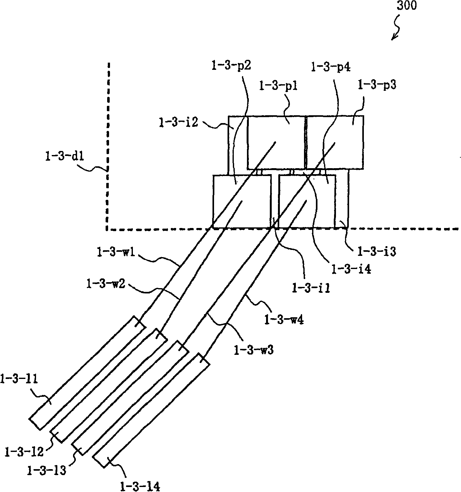
[0191] image 3 It is a partially enlarged plan view showing a semiconductor device 300 according to Embodiment 1 of the present invention corresponding to Invention 1.

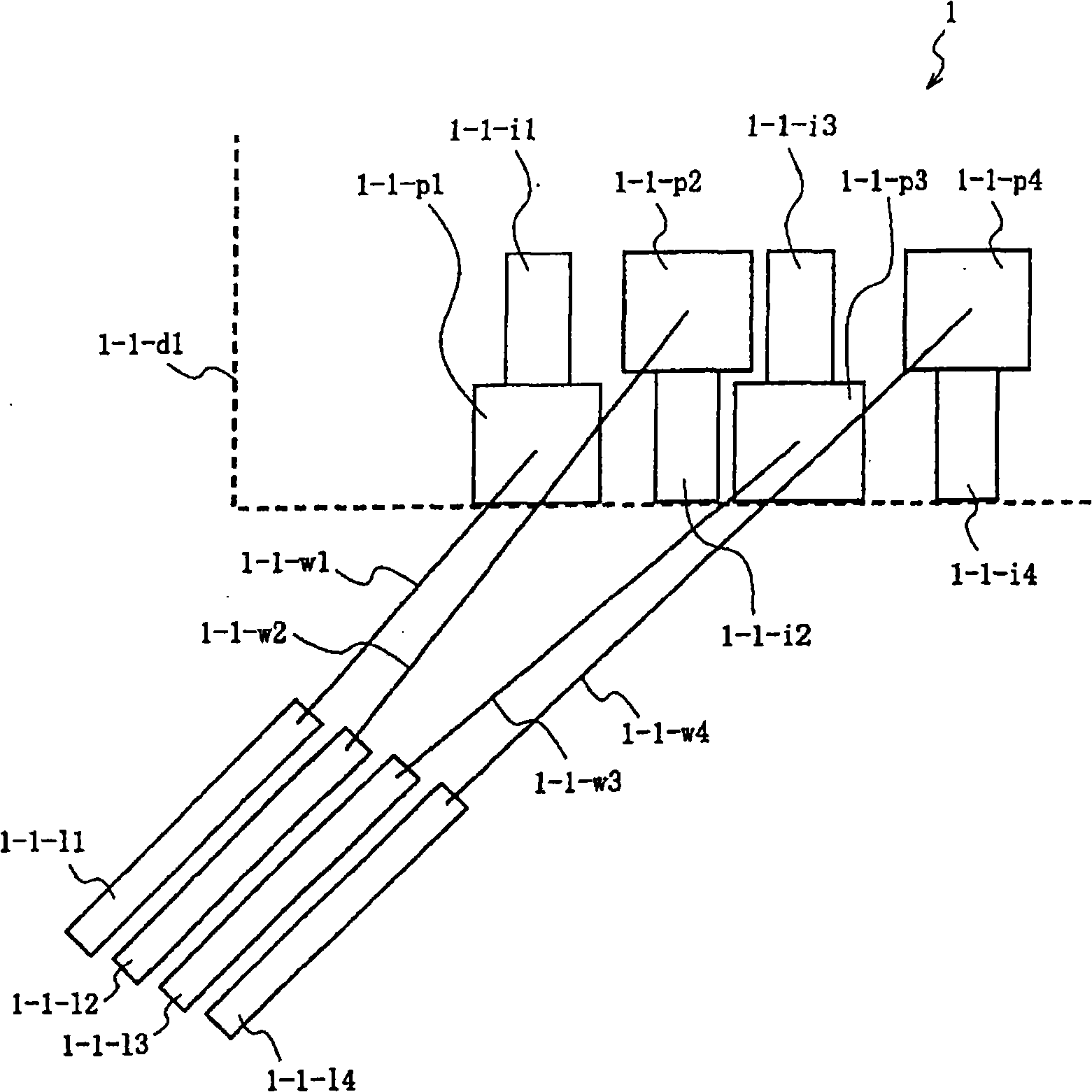
[0192] here, figure 1 is a partially enlarged plan view of a conventional semiconductor device 1, and figure 1 In the conventional semiconductor device 1, the lead terminal 1-1-l1 is connected to the pad 1-1-p1 through the wire 1-1-w1, and is connected to the inside of the semiconductor element through the IO circuit part 1-1-i1. Similarly, the lead terminal 1-1-l2 is connected to the pad 1-1-p2 via the lead wire 1-1-w2, and is connected to the inside of the semiconductor element through the IO circuit part 1-1-i2, and the lead terminal 1-1 The same is true after -l3 figure 1 connection shown.

[0193] in addition, figure 2 is...

Embodiment approach 2

[0199] Next, the semiconductor device 400 (semiconductor device 1-1) according to Embodiment 2 of the present invention will be described.

[0200] Figure 4 It is a plan view showing a semiconductor device 400 according to Embodiment 2 of the present invention corresponding to Invention 2.

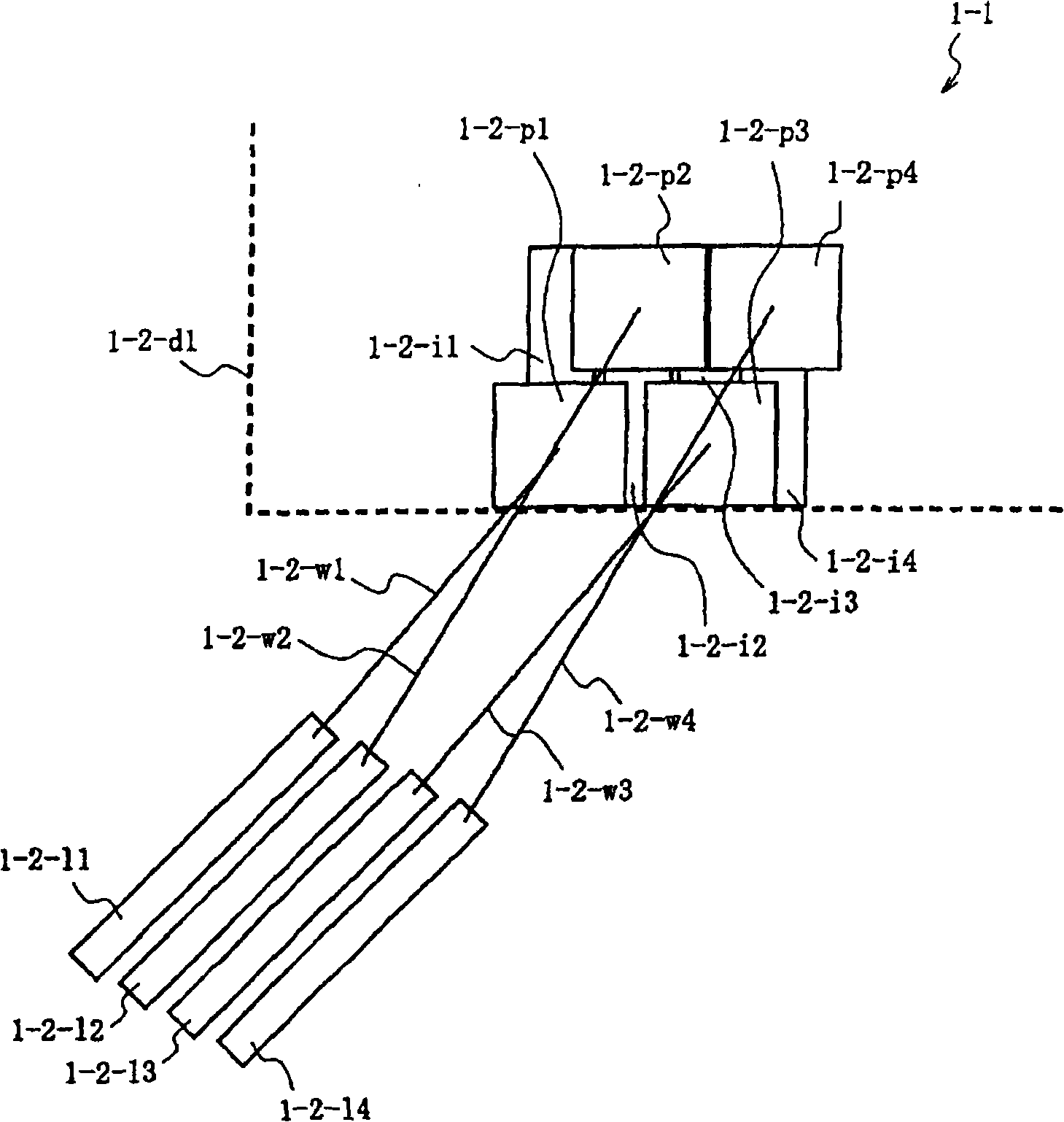
[0201] In the semiconductor device 400 of Embodiment 2, from image 3 In the shown semiconductor device 300 of Embodiment 1, the lead terminal 1-3-12 connects two wires to two pads.

[0202] Conventionally, there has been a method of connecting two wires from one lead terminal to two pads. However, in the conventional method, it is necessary to arrange the connection destination pad of the two wires adjacent to the IO circuit part so that no wire contact occurs.

[0203] exist Figure 4 In the shown semiconductor device 400 of the second embodiment, as a method of avoiding wire contact, the arrangement order of the pads and the IO circuit portion is changed.

[0204] That is, if Fi...

Embodiment approach 3

[0207] Next, a semiconductor device 500 (semiconductor device 1-2) according to Embodiment 3 of the present invention corresponding to Invention 3 will be described.

[0208] The semiconductor device 500 of the third embodiment, like the semiconductor device 400 of the second embodiment, has Figure 4 Its plan view is shown in , as the terminal function of the lead terminal 1-4-l2, the power supply or GND function is distributed, and the lead terminal 1-4-l2 is respectively connected to the soldering terminal via the wire 1-4-w2 and 1-4-w3 The pads 1-4-p2, 1-4-p3, as the IO circuit part connected to the pads 1-4-p2, 1-4-p3, configure the IO circuit as the IO circuit for power supply or GND Section 1-4-i2, 1-4-i3.

[0209] Thereby, power supply or GND can be supplied from the circuit parts 1-4-i2 and 1-4-i3 for IO of two separated positions.

[0210] In this way, in the semiconductor device 500 (semiconductor device 1-2) of the third embodiment, the terminal connecting the tw...


PUM


Abstract

Provided is a semiconductor device having staggered pad arrangement wherein pads are arranged by being alternately shifted, as a pad arrangement for connecting with an external package on an LSI. In the semiconductor device, wire short-circuit during assembly, chip size increase due to wire short-circuit prevention, propagation of power supply and GND noise due to reduction of an IO cell interval, signal transmission delay difference due to pad position shift, and the like can be eliminated. In the semiconductor device, a plurality of pads to be connected with functional terminals of the external package on the semiconductor element are arranged in two rows along the periphery of the semiconductor element. The arrangement order of the pads on the semiconductor element is different from that of the functional terminals of the external package.

Description

technical field [0001] The present invention relates to a semiconductor device, and in particular to a semiconductor design technology, a structure of a semiconductor device, and a semiconductor element. Background technique [0002] In the manufacture of semiconductor devices, there is a wire bonding method in which a pad provided in an LSI and a lead frame attached to a package are connected using fine wires. This method has been established for a long time, and is currently widely used because it is relatively easy to connect and has high reliability. In recent years, the number of pins has been increasing along with the integration of semiconductor elements and the increase in the functions of semiconductor elements. Therefore, for example, it is necessary to respectively connect dozens to hundreds of pads and lead terminals arranged along the periphery of the component with wires, and at this time, it is necessary to prevent electrical shorts caused by wires touching e...

Claims


Application Information

Patent Timeline
Patent Type & Authority Applications(China)
IPC IPC(8): H01L21/60H01L21/82H01L21/822H01L27/04
CPCH01L2224/06153H01L2924/01082H01L2924/00014H01L23/50H01L2924/01004H01L2224/49113H01L2924/01002H01L24/06H01L2224/49431H01L2224/48091H01L2224/49171H01L24/49H01L2224/4917H01L24/45H01L2224/48599H01L2924/3011H01L2224/85399H01L24/48H01L2924/01079H01L2224/48247H01L24/85H01L2224/04042H01L2924/01033H01L2924/01074H01L2224/05599H01L2924/01058H01L2224/45144H01L2224/05554H01L24/05H01L2224/023H01L2224/78H01L2924/00H01L2924/0001
Inventor 山田裕岸田武田村义一曾川泰生广藤政则
Owner PANASONIC SEMICON SOLUTIONS CO LTD
Why Eureka
Try Eureka