Substrate processing method

A substrate processing method and substrate technology, applied in the direction of electrical components, semiconductor/solid-state device manufacturing, circuits, etc., can solve problems such as disengagement, generation of particles, and inability to uniform force on the wafer, so as to reduce temperature deviation and be easy to adjust Effect

Inactive Publication Date: 2008-09-17
PSK INC
View PDF0 Cites 4 Cited by
  • Summary
  • Abstract
  • Description
  • Claims
  • Application Information

AI Technical Summary

Problems solved by technology

In the past, mechanical clamps or electrostatic chucks were used, but the mechanical clamps could not force the wafer uniformly, and had the disadvantage of generating particles
In addition, in the case of using an electrostatic chuck, the structure of the device becomes complicated, and the production cost increases. In addition, when handling, it is necessary to have a process of clamping or disengaging

Method used


Image

  • Substrate processing method
  • Substrate processing method
  • Substrate processing method

Examples


Embodiment Construction

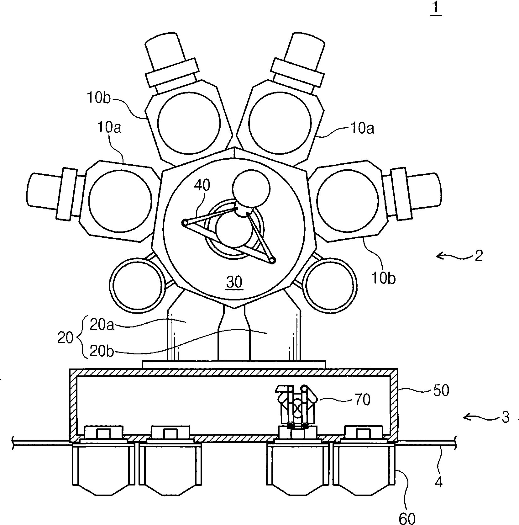
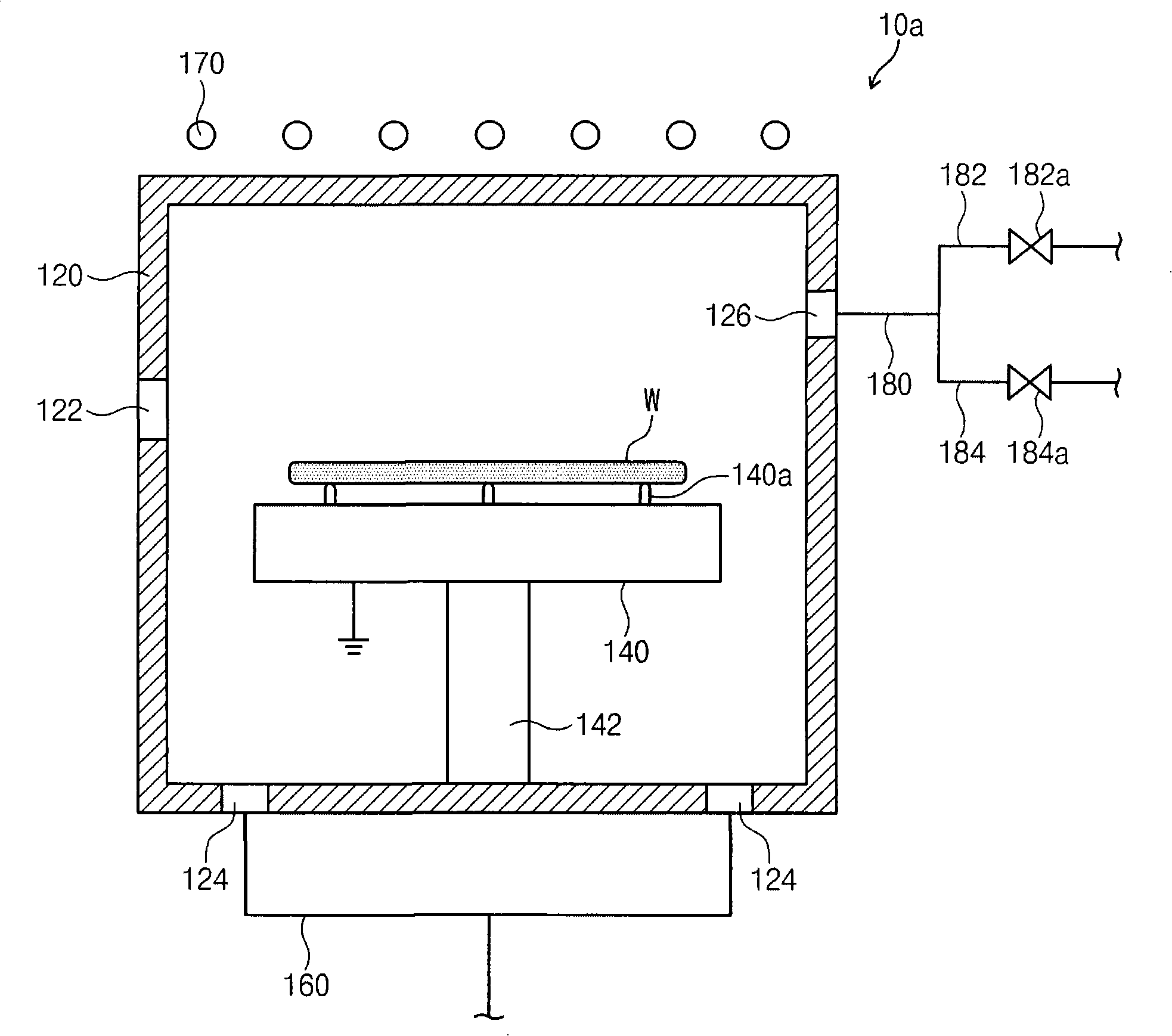
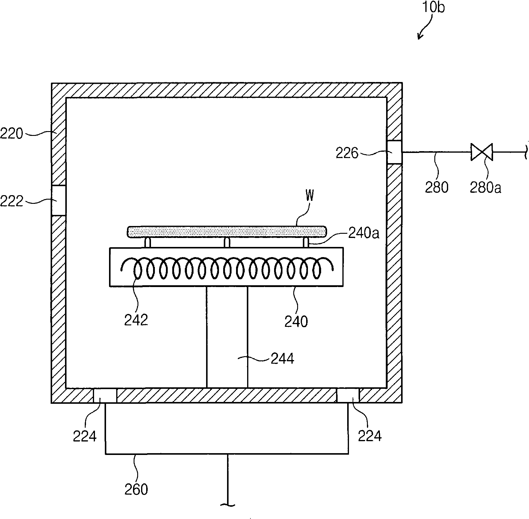
[0035] Refer below figure 1 ~ Fig. 7 is a detailed description of a preferred embodiment of the present invention. The embodiments of the present invention can be changed into various different forms, and the scope of the present invention should not be interpreted as being limited to the embodiments described later. The purpose of this embodiment is to explain the present invention in more detail to those having ordinary technical knowledge belonging to the technical field of the present invention. Therefore, in order to emphasize the description more clearly, the shapes of the elements shown in the drawings may be exaggerated.

[0036] The following describes the wafer W as an example of the substrate, but the technical idea and scope of the present invention are not limited to this. In addition, in order to explain the present invention, a plasma etching apparatus is used as an example for description below, but the present invention can be applied to various semiconductor man...


PUM


Abstract

The invention provides a substrate processing method. The substrate mounted within a processing chamber is disposed on a support anode. Then the processing chamber is isolated from outside and pressure within the processing chamber is increased to reach an established pressure under which temperature of the substrate is kept at a particular temperature, after that, pressure within the processing chamber is decreased to reach a processing pressure. The substrate is disassembled to outside of the processing chamber once the processing for substrate is accomplished in the processing chamber. The method for increasing the pressure within the processing chamber comprises the methods for provision of purification gases and processing gases.

Description

Technical field [0001] The present invention relates to a method for processing a substrate, and more particularly to a method for processing a substrate placed on an anode (plate). Background technique [0002] The film deposited on the surface of the wafer can be selectively removed by etching, and a desired pattern is formed on the surface of the wafer. This process is repeated in the semiconductor manufacturing process. In addition, not only for the vapor-deposited film, but also for forming trenches, the silicon substrate itself may be etched. The thin film may include different thin films such as photoresist, silicon oxide film, or silicon nitride film. An oxide film or a nitride film will provide better etching conditions than a photoresist. [0003] Next, a general plasma etching apparatus will be described. The processing gas is supplied into the chamber, and once an electric field is formed between the two electrodes, a part of the gas atoms are ionized to generate cati...

Claims


Application Information

Patent Timeline
Patent Type & Authority Applications(China)
IPC IPC(8): H01L21/00H01L21/3065C23F4/00
CPCH01L21/02046H01L21/3065
Inventor 金镇佑
Owner PSK INC
Why Eureka
Try Eureka