Method for making strain silicon CMOS transistor

An oxide semiconductor, complementary technology, applied in semiconductor/solid-state device manufacturing, electrical components, circuits, etc., can solve problems such as PMOS damage, PMOS transistor damage, PMOS transistor drive current drop, etc., to improve operating performance and ensure reliability Acceleration, the effect of increasing the drift rate

Inactive Publication Date: 2008-09-17
UNITED MICROELECTRONICS CORP
View PDF0 Cites 10 Cited by
  • Summary
  • Abstract
  • Description
  • Claims
  • Application Information

AI Technical Summary

Problems solved by technology

Under this environment, the lattice spacing in the channel of the NMOS transistor increases, which is conducive to the movement of electrons in the channel, and the carrier mobility of the NMOS transistor also increases. The expected improvement effect is achieved; however, in contrast to the PMOS transistor, the tensile stress covering the surface of the PMOS transistor not only fails to improve the performance of the PMOS transistor, but also causes a sharp drop in the driving current of the PMOS transistor, causing negative damage to the PMOS; on the other hand , if the surface of the CMOS transistor is covered with a film of high compressive stress, although it can effectively improve the performance of the NMOS transistor, it will also cause damage to the PMOS transistor. The technology of generating channel strain in the known technology has a great impact on how to improve the performance of NMOS transistors and PMOS transistors thus caught in a dilemma

Method used


Image

  • Method for making strain silicon CMOS transistor
  • Method for making strain silicon CMOS transistor
  • Method for making strain silicon CMOS transistor

Examples


Embodiment Construction

[0024] In order to highlight the advantages and features of the present invention, a number of preferred embodiments of the present invention are listed below, and are described in detail in conjunction with the drawings as follows:

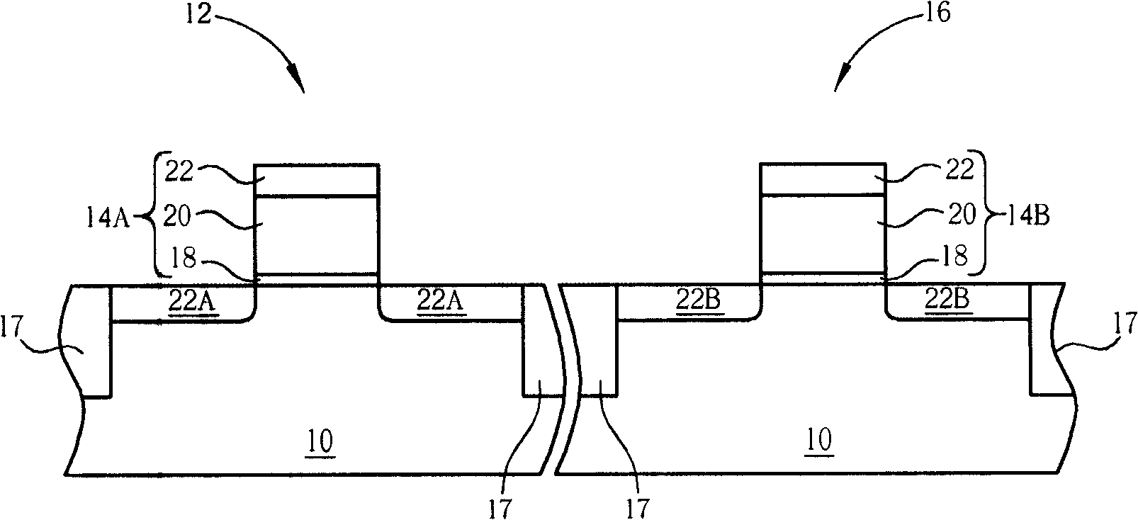
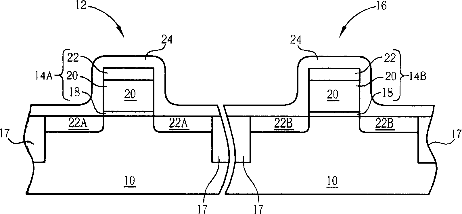
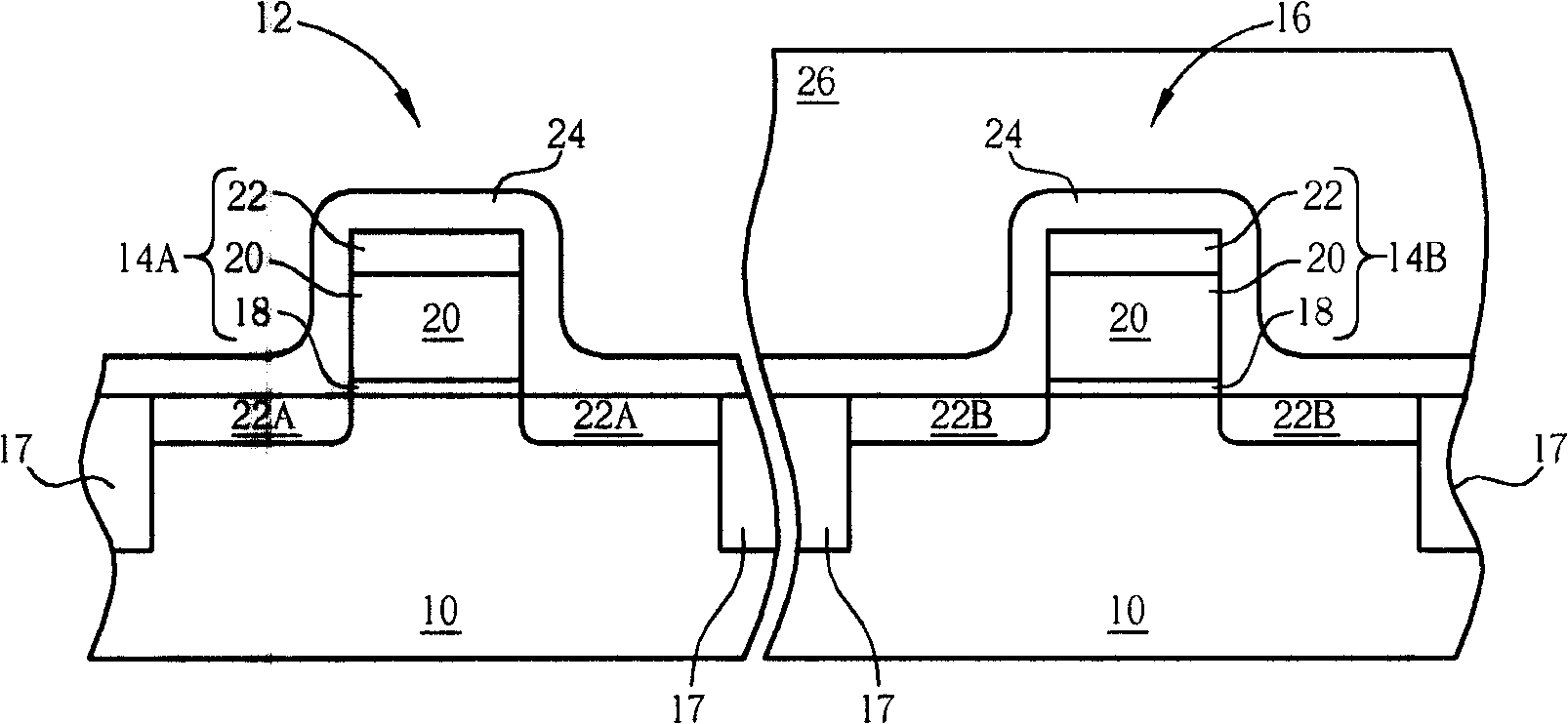
[0025] Please refer to Figure 1 to Figure 7 , Figure 1 to Figure 7 It is a schematic diagram illustrating each step of manufacturing a strained silicon CMOS transistor according to the first preferred embodiment of the present invention. Such as figure 1 As shown, firstly, a semiconductor substrate 10 is provided, and the semiconductor substrate 10 can be silicon, a strained silicon substrate, a compound semiconductor, a silicon-on-insulator substrate or a combination thereof. The semiconductor substrate 10 can be individually formed on the semiconductor substrate 10 by methods known to those skilled in the art, such as masking process, ion implantation process and rapid thermal annealing (rapid thermal annealing, hereinafter referred to as RT...


PUM


Abstract

A method for manufacturing a strained silicon CMOS (complementary metal oxide semiconductor) comprises: first providing a semiconductor substrate, the semiconductor substrate comprises at least a first active area and at least a second active area; then forming a high-stress film to cover the semiconductor substrate, the first active area and the second active area; then forming a mask to cover part of the high-stress film over the first active area; then carrying out ion implantation process, in order to implant dopant into part of the high-stress film disposed on the second active area and not covered by the mask, and adjust the stress factor thereof; then removing the mask and carrying out a rapid annealing process; finally, removing the high-stress film to realize the invention.

Description

technical field [0001] The present invention relates to a method for manufacturing a strained silicon complementary metal-oxide semiconductor (complementary metal-oxide semiconductor, hereinafter referred to as CMOS) transistor, in particular to a method for covering a high-stress film on a CMOS transistor, and using an ion implantation process to adjust the high-stress film The stress number can effectively improve the manufacturing method of the strained silicon CMOS transistor which can effectively improve the operating performance of the CMOS transistor. Background technique [0002] In recent years, the use of shrinking device size to improve the performance of metal-oxide semiconductor (hereinafter referred to as MOS) transistors has been affected by negative factors such as lithography technology bottlenecks and high costs. The industry has begun to seek other methods. To improve the operating performance of MOS transistors, the method of using material properties to ...

Claims


Application Information

Patent Timeline
Patent Type & Authority Applications(China)
IPC IPC(8): H01L21/8238H01L21/3105
Inventor 陈哲明陈能国廖秀莲蔡腾群
Owner UNITED MICROELECTRONICS CORP
Why Eureka
Try Eureka