Metal silication technique for metal-oxide-semiconductor transistor and transistor construction

An oxide semiconductor and metal silicidation technology, which is applied in semiconductor devices, semiconductor/solid-state device manufacturing, electrical components, etc., can solve the problems of difficult control, complicated chemical mechanical polishing process steps, etc., and achieve the effect of easy control and simple process

Inactive Publication Date: 2008-10-01
UNITED MICROELECTRONICS CORP
View PDF0 Cites 4 Cited by
  • Summary
  • Abstract
  • Description
  • Claims
  • Application Information

AI Technical Summary

Problems solved by technology

However, the steps of the chemical mechanical polishing process are quite complicated and difficult to control

Method used


Image

  • Metal silication technique for metal-oxide-semiconductor transistor and transistor construction
  • Metal silication technique for metal-oxide-semiconductor transistor and transistor construction
  • Metal silication technique for metal-oxide-semiconductor transistor and transistor construction

Examples


Embodiment Construction

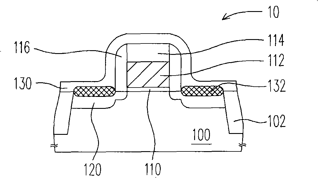
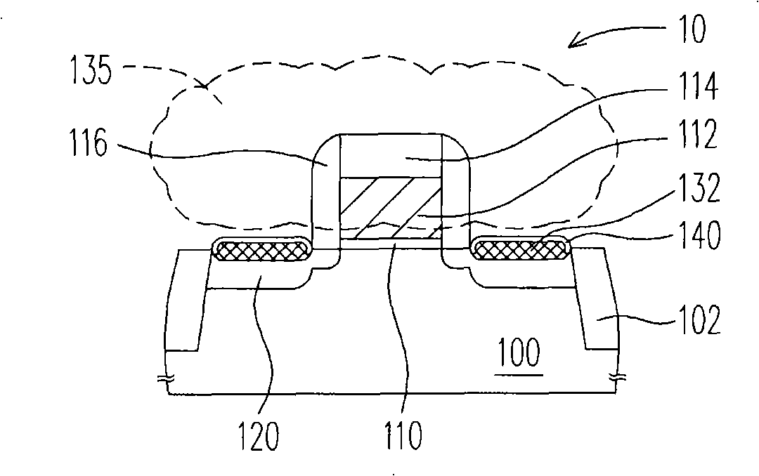
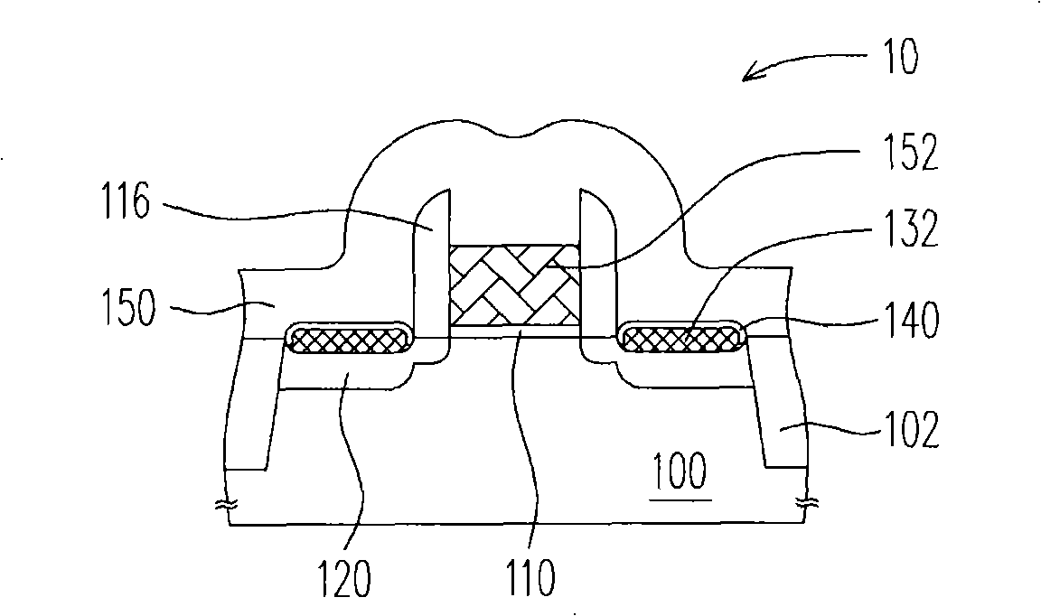
[0026] Figure 1~3 A cross-sectional flow diagram illustrating a metal silicide process for a metal oxide semiconductor transistor according to a preferred embodiment of the present invention.

[0027] Please refer to figure 1 , first provide a metal oxide semiconductor transistor 10, which includes a silicon substrate 100 formed with an isolation layer 102, a gate dielectric layer 110 on the silicon substrate 100, a silicon gate 112 on the gate dielectric layer 110, and a silicon gate 112 on the silicon gate 112. The top cap layer 114 , the spacer 116 between the silicon gate 112 and the sidewall of the top cap layer 114 , and the source / drain region 120 in the substrate 100 next to the silicon gate 112 . Wherein, the silicon substrate 100 is, for example, a lightly P-type or lightly N-type doped silicon substrate, the gate dielectric layer 110 is, for example, a gate oxide layer, and the material of the silicon gate 112 is, for example, polysilicon.

[0028] In addition, t...


PUM


Abstract

The invention relates to a metal silicatization process for metal oxide semiconductor transistor, and a transistor structure formed by the process, wherein the metal oxide semiconductor transistor comprises a silicon substrate, a grid dielectric layer, a silicon grid electrode, a top cover layer on the silicon grid electrode, a gap wall between the silicon grid electrode and sidewall of the top cover layer, and source / drain electrode areas in the substrate next to the silicon grid electrode. The process comprises the steps of forming a metal silicide layer on the source / drain electrode areas, removing the top cover layer and reacting the silicon grid electrode to the full-metal silicide grid electrode, characterized in that plasma of reactive gas is utilized to react the surface layer of the metal silicide layer so as to form a protective layer after forming the metal silicide layer and before removing the top cover layer.

Description

technical field [0001] The present invention relates to a semiconductor process and a structure of a semiconductor element, and in particular to a silicidation process of a metal oxide semiconductor transistor (MOS transistor) and a transistor structure formed by the process. Background technique [0002] In the metal oxide semiconductor transistor (MOS transistor) process in recent years, in order to reduce the resistance of the source / drain and the silicon gate, a so-called salicide process is generally performed. The traditional self-aligned metal silicide process is to cover a layer of refractory metal (refractory metal) on the transistor first, and then heat the silicon material on the surface of the source / drain region and the gate to react with the metal to form a metal silicide, and then remove Unreacted metal. [0003] However, as the size of semiconductor devices shrinks day by day, the resistance of the gate must be further reduced. One of the methods is to make ...

Claims


Application Information

Patent Timeline
IPC IPC(8): H01L21/336H01L21/28H01L29/78H01L29/43H01L29/49
Inventor 谢朝景张毓蓝黄建中洪宗佑张俊杰陈意维
Owner UNITED MICROELECTRONICS CORP
Why Eureka
Try Eureka