Method for preparing light inductor

A light sensor, light sensing technology, applied in semiconductor/solid-state device manufacturing, electrical components, circuits, etc., can solve the problems of photocurrent attenuation, low photocurrent stability, and the inability of light sensors to meet the application, and improve reliability. the effect of reducing the cost of the manufacturing process

Active Publication Date: 2008-10-08
AU OPTRONICS CORP
View PDF0 Cites 20 Cited by
  • Summary
  • Abstract
  • Description
  • Claims
  • Application Information

AI Technical Summary

Problems solved by technology

However, amorphous silicon thin film transistor sensors have the disadvantage of low photocurrent stability, and even when the sensor is not operated, the photocurrent decays over time, so there is a serious reliability problem
[0003] Based on the above reasons, the photosensors currently used in the industry can no longer meet its application in the field of optoelectronics, so a new generation of photosensors has become the focus of research and development

Method used


Image

  • Method for preparing light inductor
  • Method for preparing light inductor
  • Method for preparing light inductor

Examples


Embodiment Construction

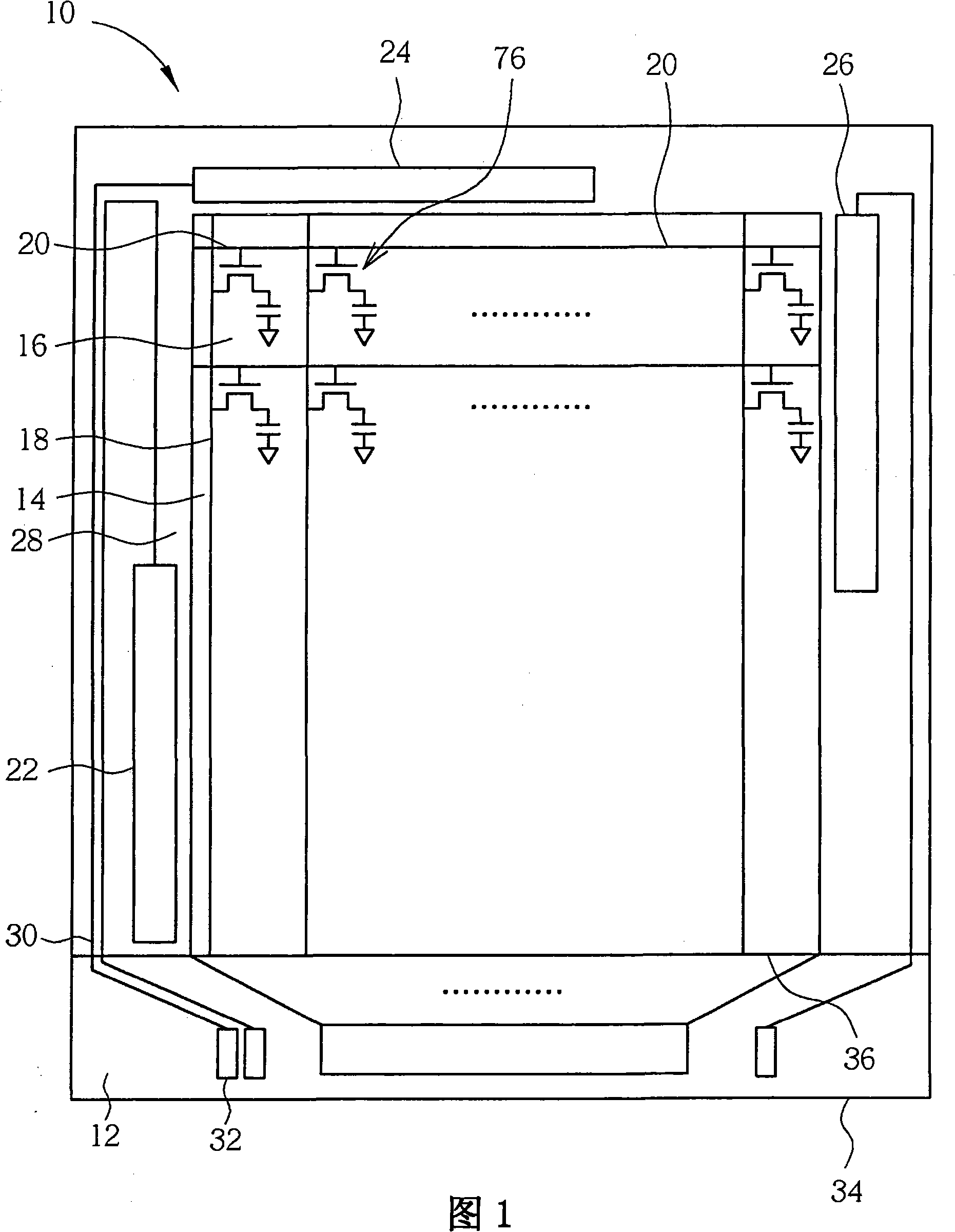
[0051] Please refer to FIG. 1 . FIG. 1 is a schematic diagram of applying the light sensor of the present invention to an amorphous silicon TFT display panel. The amorphous silicon TFT display panel 10 includes a lower substrate 34 and an upper substrate 36. When the amorphous silicon TFT display panel 10 is a liquid crystal display panel, the lower substrate 34 and the upper substrate 36 are usually called an array substrate and a color filter substrate respectively. . However, the TFT display panel 10 can also be other types of flat display panels, such as organic light emitting display panels. The amorphous silicon TFT display panel 10 further includes a display area 14 and a peripheral circuit area 12, wherein a plurality of scanning lines 20 and signal lines 18 are arranged in the display area 14, defining pixels 16 arranged in an array, and each pixel 16 includes A TFT device 76 is electrically connected to the scan line 20 and the signal line 18 . In addition, the TFT...


PUM


Abstract

A method for preparing an optical inductor includes steps: providing a substrate comprising a thin film transistor region and an optical induction region; forming a patterned first conductive layer on the substrate; forming a grid dielectric layer on surface of the substrate and a grid; forming a patterned amorphous silicon layer on surface of the grid dielectric layer which is deposed on the grid; forming a patterned second conductive layer on the substrate; forming a patterned silicon-enriched dielectric layer on the substrate; forming a patterned light-transparent conductive layer on the substrate which at least comprises an upper electrode of the optical inductor and is arranged in the optical induction region. The optical inductor includes a bottom electrode, a dielectric layer comprising silicon-enriched material and the upper electrode. The method of present invention can effectively increase reliability of the optical inductor and reduce whole preparation cost of products by integrating thin film transistor preparation technique.

Description

technical field [0001] The present invention relates to a method for fabricating a photosensor for an amorphous silicon thin film transistor (thin filmtransistor, TFT) panel, especially a photosensor for fabricating a silicon-rich (Si-rich) dielectric material. The device is used in the method of amorphous silicon thin film transistor panel. Background technique [0002] Photosensors have gradually been widely used in various types of TFT displays. The current photosensors are mainly PIN (p-intrinsic-n) diodes (photodiodes) formed of materials from the three-A group and the five-A group. However, the PIN diode The light receiving efficiency is low, and it is easily affected by non-target light sources, so it has disadvantages such as poor signal-to-noise ratio. In addition, for TFT displays, the three-A and five-A materials used in PIN diodes are also compatible with the TFT manufacturing process. Therefore, traditional PIN diodes have their development limitations in terms...

Claims


Application Information

Patent Timeline
Patent Type & Authority Applications(China)
IPC IPC(8): H01L21/84
Inventor 石靖节卓恩宗彭佳添林昆志
Owner AU OPTRONICS CORP
Why Eureka
Try Eureka