
Integration process flow for flash devices with low gap fill aspect ratio

A technology of isolation structure and shallow trench, applied in the process of forming it, the structure of memory cells and the field of memory cell arrays

Active Publication Date: 2011-03-30
SANDISK TECH LLC
View PDF4 Cites 1 Cited by
  • Summary
  • Abstract
  • Description
  • Claims
  • Application Information

AI Technical Summary

Problems solved by technology

Pitting tends to only occur for larger recesses so that it may not affect the memory array, but may be noticeable for peripheral areas with large features

Method used


Image

  • Integration process flow for flash devices with low gap fill aspect ratio
  • Integration process flow for flash devices with low gap fill aspect ratio
  • Integration process flow for flash devices with low gap fill aspect ratio

Examples


Embodiment Construction

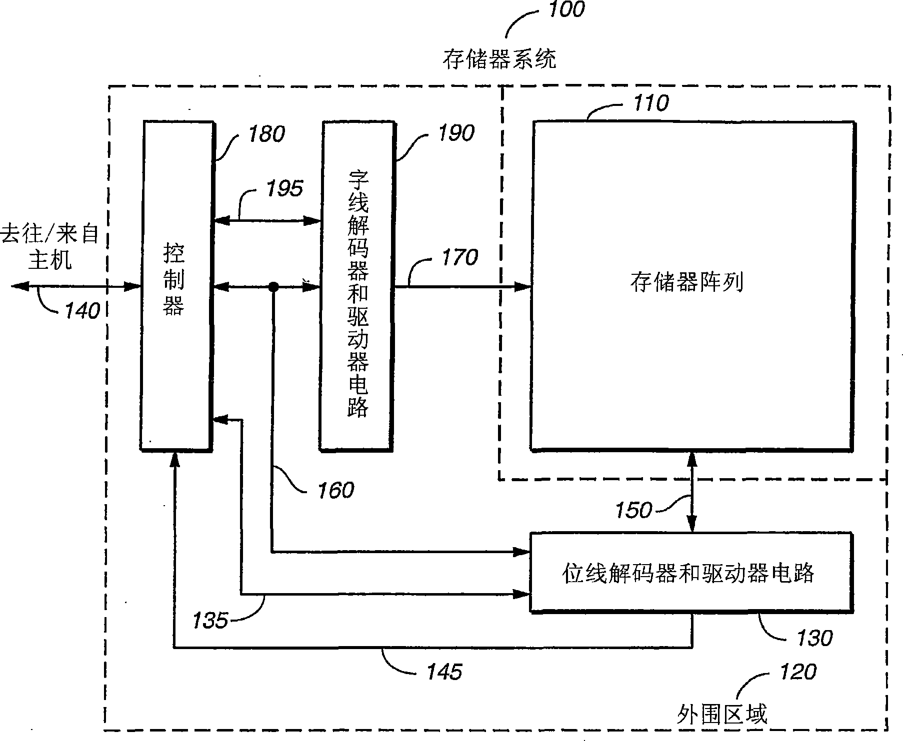
[0037] exist figure 1 An example of a memory system 100 incorporating various aspects of the present invention is generally illustrated in the block diagram of . A large number of individually addressable memory cells are arranged in a regular array of rows and columns 110, although other physical cell arrangements are of course possible. It is specified here that the bitlines extending along the columns of the array 110 are electrically connected to the bitline decoder and driver circuit 130 by lines 150 . Wordlines specified in this description to extend along a row of array 110 are electrically connected to wordline decoder and driver circuit 190 by line 170 . Each of decoders 130 and 190 receives memory cell addresses from memory controller 180 over bus 160 . The decoder and driver circuits are also connected to the controller 180 via respective control and status signal lines 135 and 195 .

[0038] The controller 180 can be connected to a host device (not shown) throu...


PUM


Abstract

A non-volatile memory is formed having shallow trench isolation structures between floating gates and having control gates extending between floating gates where shallow trench isolation dielectric is etched. Control of etch depth is achieved using ion implantation to create a layer of dielectric with a high etch rate compared with the underlying dielectric. A conductive layer overlies the substrate during implantation. A substrate having small polysilicon features in a memory array and large polysilicon features in a peripheral area is accurately planarized using protrusions in the peripheral area and a soft chemical mechanical polishing step that stops when protrusions are removed.

Description

technical field [0001] The present invention relates generally to non-volatile flash memory systems, and more particularly to structures of memory cells and arrays of memory cells, and processes for forming the same. Background technique [0002] There are many commercially successful non-volatile memory products in use today, especially in the form of small form factor cards, which use arrays of flash EEPROM (Electrically Erasable Programmable Read Only Memory) cells. These cards can be interfaced with the host, for example, by removably inserting the card into a card slot in the host. Some cards available for purchase are CompactFlash TM (CF) Card, MultiMediaCard (MMC), Secure Digital (SD) Card, SmartMedia, Personal Tag (P-Tag) and Memory Stick Card. Hosts include personal computers, notebook computers, personal digital assistants (PDAs), various data communication devices, digital cameras, cellular phones, portable audio players, car audio systems, and similar types of ...

Claims


Application Information

Patent Timeline
Patent Type & Authority Patents(China)
IPC IPC(8): H01L21/762H01L21/8239H01L21/8247H01L21/311H01L27/115H01L27/105H10B69/00H10B99/00
CPCH01L27/11531H01L21/3212H01L21/31111H01L27/115H01L27/105H01L27/11526H01L27/1052H10B69/00H10B41/40H10B41/42
Inventor 图安·D·法姆东谷正昭
Owner SANDISK TECH LLC
Learn More