Method for reinforcing MOS device channel region strain

A technology for MOS devices and channel regions, applied in semiconductor/solid-state device manufacturing, electrical components, circuits, etc., can solve problems such as high cost, low cost, complex process, etc., to improve performance, increase strain, and improve device performance Effect

Inactive Publication Date: 2008-10-29
TSINGHUA UNIV
View PDF0 Cites 57 Cited by
  • Summary
  • Abstract
  • Description
  • Claims
  • Application Information

AI Technical Summary

Problems solved by technology

Generally speaking, the former introduces a greater degree of strain, but the process is more complicated and the cost is higher; while the latter has a small strain and the performance of the device is limited, but the process is simple and the cost is low, and it has been applied in industrial production.

Method used


Image

  • Method for reinforcing MOS device channel region strain
  • Method for reinforcing MOS device channel region strain
  • Method for reinforcing MOS device channel region strain

Examples


Embodiment 1

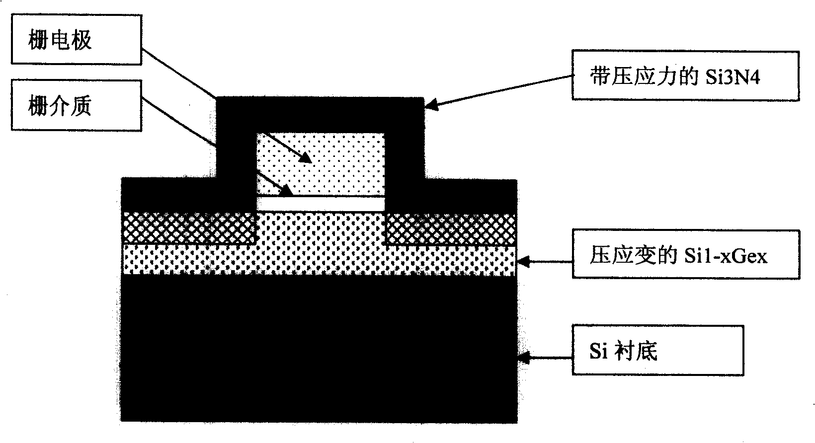
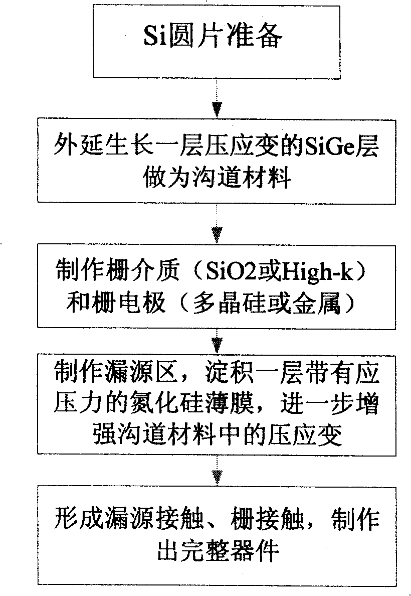
[0022] Embodiment 1: PMOS transistor with SiGe channel. A layer of compressively strained SiGe is epitaxially used as the channel layer on the silicon substrate, and a layer of High-k dielectric is deposited on it by ALD as the gate dielectric, and then a metal gate is deposited, and then a layer of nitrogen with compressive stress is deposited. Si 3 N 4 The strain degree of the channel layer is further enhanced to improve performance (in Example 1).

Embodiment 2

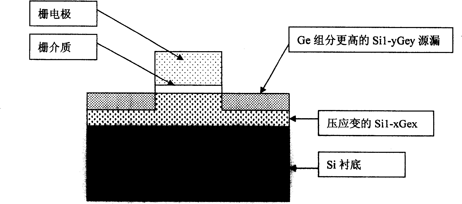
[0023] Embodiment 2: PMOS transistor with SiGe channel. A layer of strained SiGe is epitaxially used as the channel layer on the silicon substrate, and a layer of High-k dielectric is deposited on it by ALD as the gate dielectric, and then the metal gate is deposited, and then the source and drain are etched to remove the SiGe in the source and drain regions , and then grow a silicon germanium layer with a higher Ge content in the source and drain regions, squeeze the channel region material, and further introduce compressive stress in the channel to enhance strain and improve performance.

Embodiment 3

[0024] Embodiment 3: CMOS process on SOI composed of SIGe material PMOS and strained silicon NMOS. First, use Bonding or other methods to obtain a high-quality relaxed SiGe layer on the insulating layer as a virtual substrate, and then define a certain area on it by photolithography, and epitaxially grow a compressively strained SiGe layer with higher Ge content As the PMOS tube area, a layer of tensile strained Si layer is deposited in other areas as the NMOS tube area, and STI is used to isolate the two areas. PMOS transistors and NMOS transistors are fabricated in two regions respectively. Then deposit a layer of Si with compressive stress on the PMOS tube 3 N 4 The thin film introduces greater compressive stress in the channel region, and deposits a layer of Si with tensile stress on the NMOS tube. 3 N 4 The thin film introduces greater tensile stress in the NMOS channel region, so that high-performance PMOS tubes and NMOS tubes can be obtained at the same time, formin...


PUM


Abstract

The invention discloses a method for further improving the strain degree of a groove material, improving the transferring rate and enhancing the strain of the groove area of an MOS apparatus for enhancing the apparatus properties. The technical scheme is that: a method for enhancing the strain of the groove area of the MOS apparatus is characterized by including the following steps of: extending an SiGe layer with gradient components on a silicon underlay; then extending a Ge layer or an Si layer to obtain a strained groove material layer and then inducing a large strain through a technique method to further improve the strain degree of the material and improve the apparatus properties.

Description

technical field [0001] The present invention relates to the field of methods for introducing strain into a channel material of a semiconductor substrate. A strained channel material layer is obtained by epitaxially extending a SiGe layer with a graded composition on a silicon substrate, and then epitaxially extending a germanium layer or a silicon layer. Then, a greater stress is introduced through the process method to further increase the strain degree of the material and improve the performance of the device. The method for enhancing the strain in the channel region of the MOS device of the invention can be used in the strained silicon or germanium process in the CMOS process to further increase the strain degree of the channel material, increase the mobility, and enhance the performance of the device. Background technique [0002] As feature sizes get smaller and smaller, integrated circuits face many small size effects caused by materials and devices themselves. The co...

Claims


Application Information

Patent Timeline
Patent Type & Authority Applications(China)
IPC IPC(8): H01L21/336H01L21/20H01L21/8238H01L21/84
Inventor 郭磊王敬许军刘佳磊梁仁荣刘志弘
Owner TSINGHUA UNIV
Why Eureka
Try Eureka