

Semiconductor device
A technology of semiconductors and bumps, which is applied in the direction of semiconductor devices, semiconductor/solid-state device parts, electric solid-state devices, etc., and can solve the problems of deformation, distortion, enlargement, and high contact resistance of the connecting part.
Inactive Publication Date: 2010-12-01
HITACHI LTD
View PDF4 Cites 0 Cited by
- Summary
- Abstract
- Description
- Claims
- Application Information
AI Technical Summary
Problems solved by technology
In Patent Document 1, the load at the time of connection can be absorbed by deforming the front end of the bump, but since it is a contact connection, it is not suitable for the connection between parts with different linear expansion coefficients because the contact resistance becomes high.
In addition, since heating at 150°C to 400°C is required, the deformation and distortion of the connection portion due to the difference in the linear expansion coefficient become large, and there are problems in the connection between different parts.
Method used
View moreImage
Smart ImageViewing Examples

Examples
Embodiment 1
Embodiment 2
Login to View More PUM
 Abstract
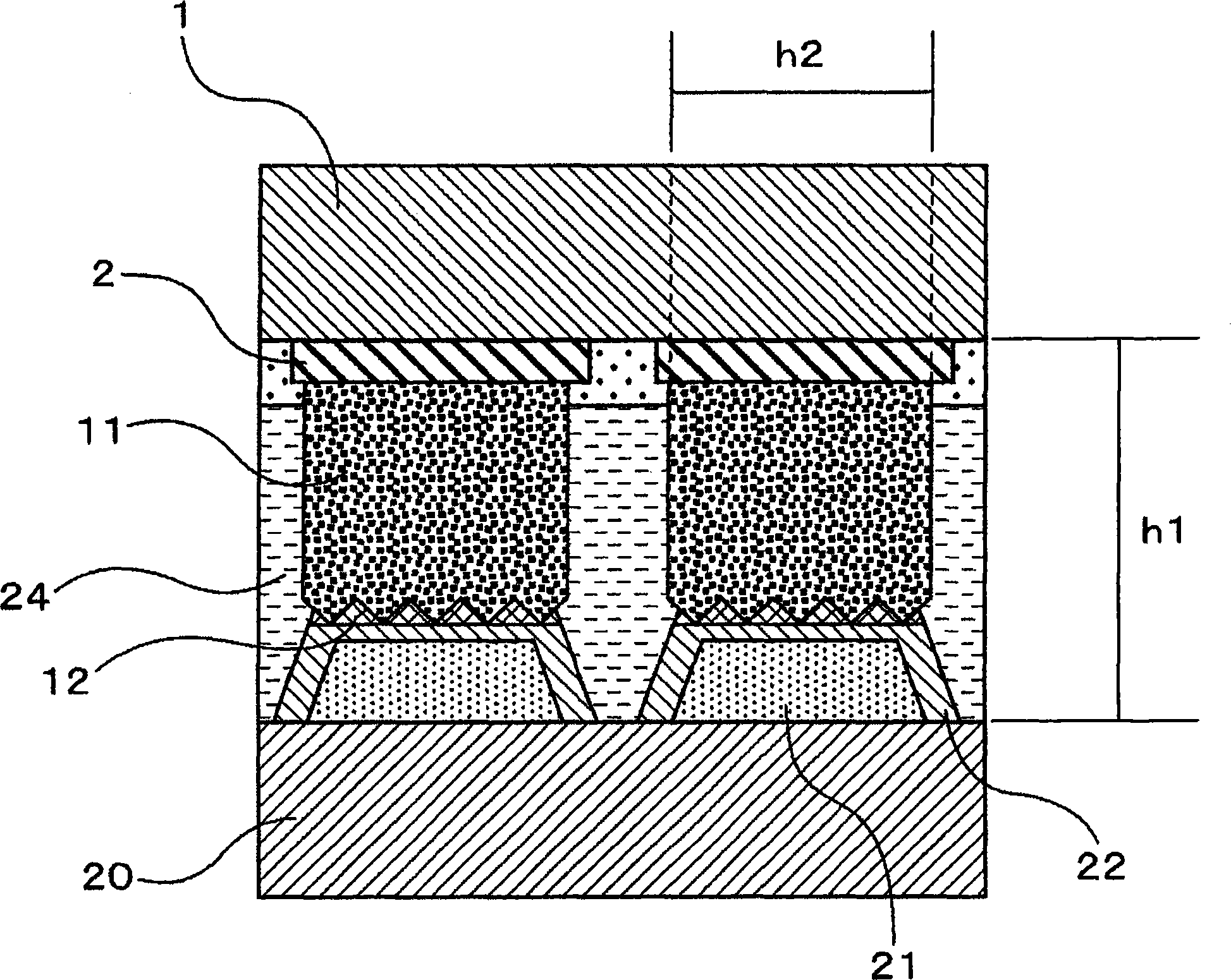
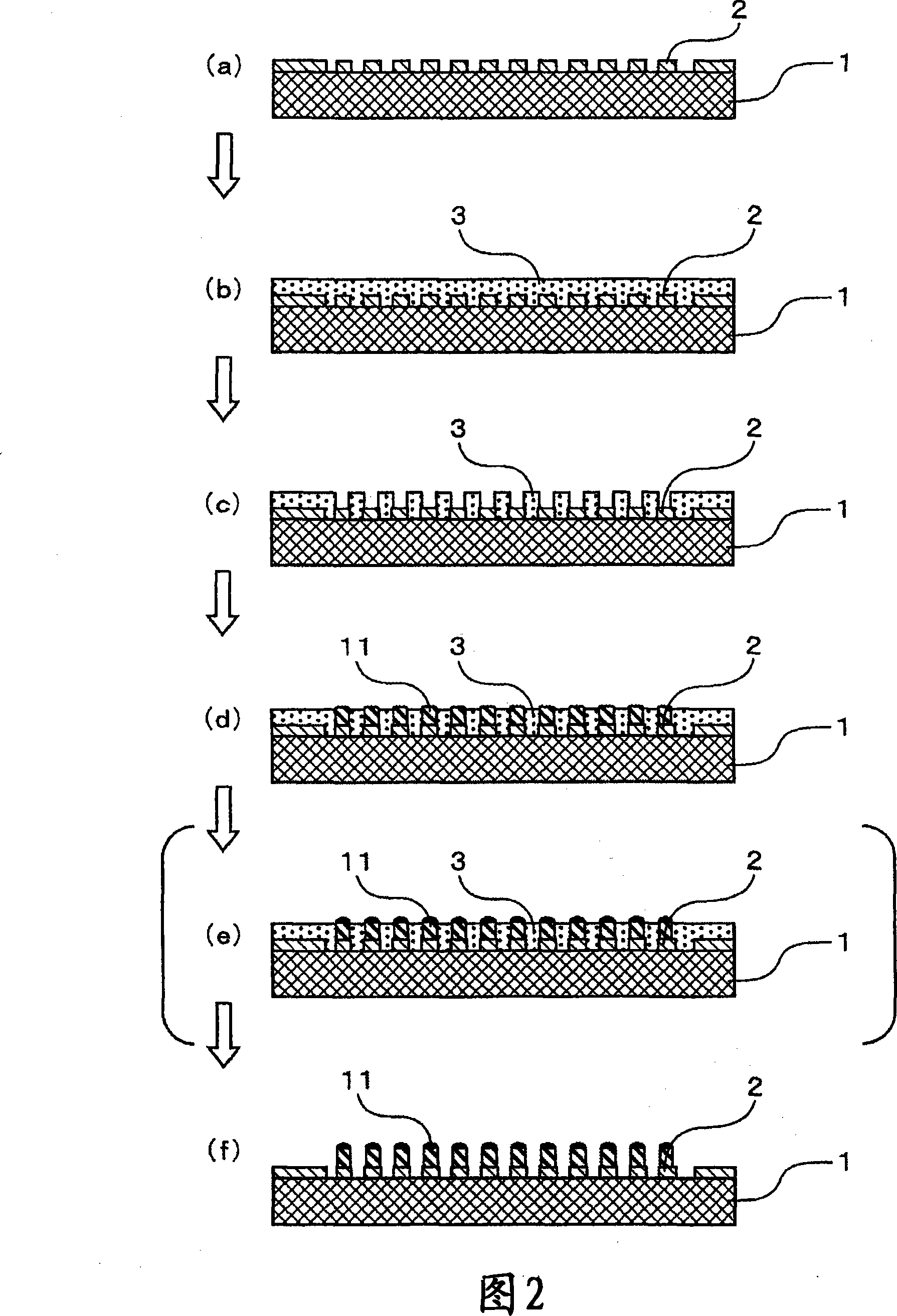
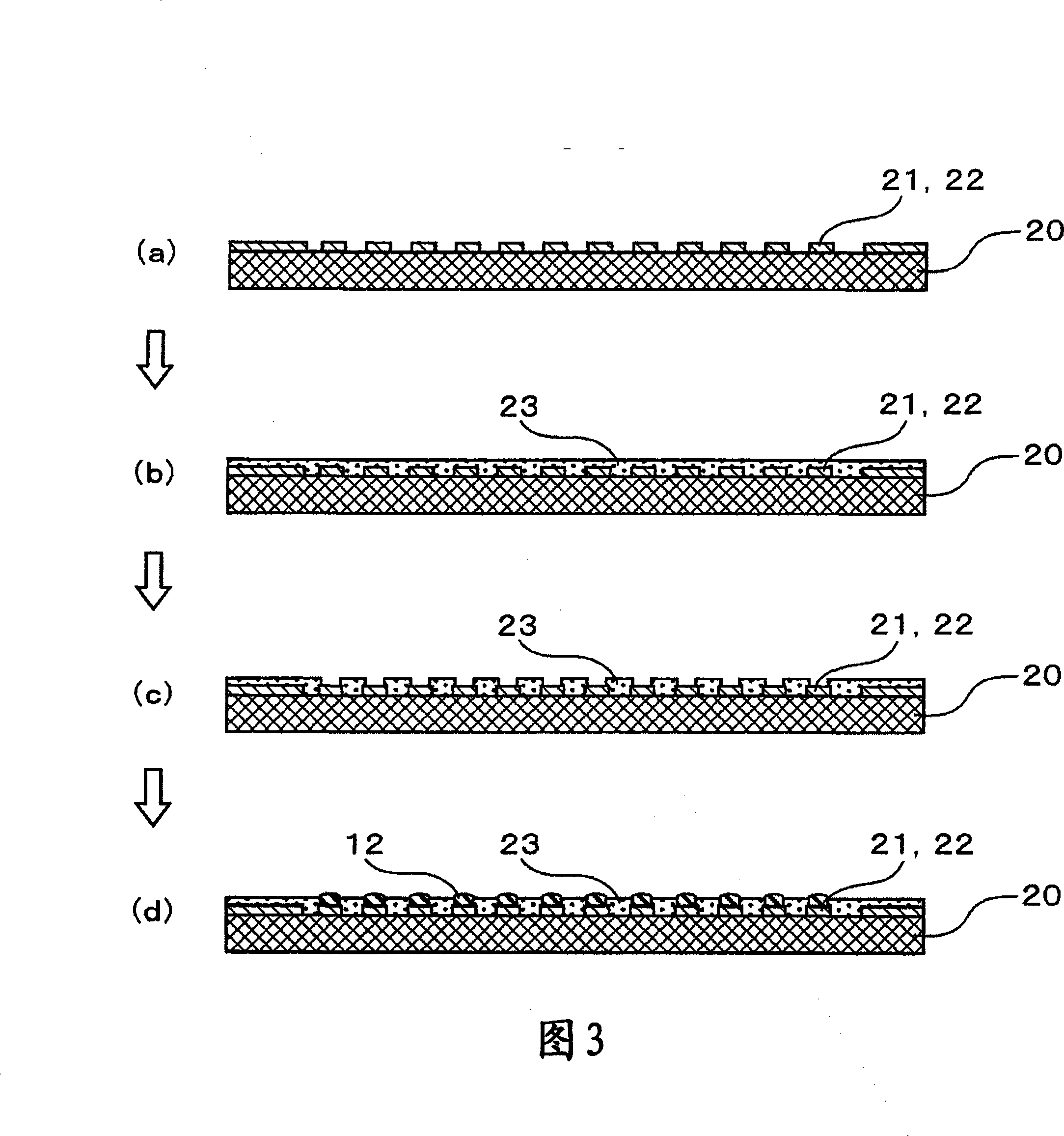
In a structure for connecting a semiconductor element having a fine pitch electrode at 50 [mu]m pitch or less and a pad or wirings on a substrate, for preventing inter-bump short-circuit or fracture of a connected portion due to high strain generated upon heating or application of load during connection, the substrate and the semiconductor element are connected by way of a bump having a longitudinal elastic modulus (Young's modulus) of 65 GPa or more and 600 GPa or less and a buffer layer including one of tin, aluminum, indium, or lead as a main ingredient and, further, protrusions are formedto at least one of opposing surfaces of the bump and the pad or the wirings on the substrate to each other, and the surfaces are connected by ultrasonic waves.
Description
Semiconductor device This application is based on and claims priority from prior Japanese patent applications JP2007-100777 filed on April 6, 2007 and JP2007-299110 filed on November 19, 2007, which are incorporated herein in their entirety The contents are for reference. technical field The present invention relates to a semiconductor device used for home appliances, consumer equipment, and industry. Background technique The demand for higher functionality centered on portable electronic devices is increasing year by year, and the accompanying high-speed and large-capacity semiconductor devices are becoming necessary. On the other hand, the miniaturization of equipment is also becoming a big demand, so that the development of these coexisting semiconductor packages is in progress. As a key technology for realizing this, flip-chip mounting, in which semiconductor elements are connected using protruding bumps, has attracted attention and has been used in various packages...
Claims
Login to View More Application Information
Patent Timeline
 Patent Type & AuthorityPatents(China)
IPC IPC(8): H01L23/488
CPCH01L2924/01013H01L2924/381H01L2924/0105H01L2924/01029H01L2224/73204H01L2224/16H01L2924/01022H01L2224/32225H01L2924/01078H01L2924/01049H01L2924/01079H01L2224/16225H01L2924/1461
Inventor藤原伸一
OwnerHITACHI LTD