

Semiconductor device, and method for fabricating thereof
A semiconductor and device technology, applied in the field of semiconductor devices, can solve the problems of insulating layer damage, reducing the reliability and loss of SONOS components
- Summary
- Abstract
- Description
- Claims
- Application Information
AI Technical Summary
Problems solved by technology
Method used
Image

Examples
Embodiment Construction
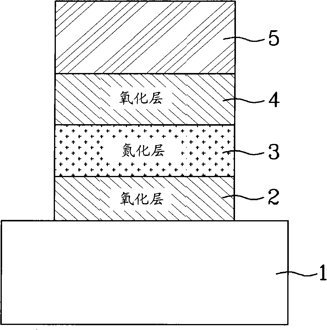
[0035] Below, the configuration and function of the embodiments of the present invention will be described with reference to the accompanying drawings. The configuration and function of the present invention shown in the accompanying drawings and described with reference to the accompanying drawings will be described by at least one embodiment. The above-mentioned technical idea of the present invention And core structure and function are not limited to this. The semiconductor device according to the present invention is a SONOS structure. Thus, the basic structure of the semiconductor device according to the present invention is that an ONO film as a plurality of insulating films laminated is formed on an upper portion of an active region, and a gate electrode is formed on an upper portion of the ONO film. And, a source / drain junction is formed in the semiconductor substrate.
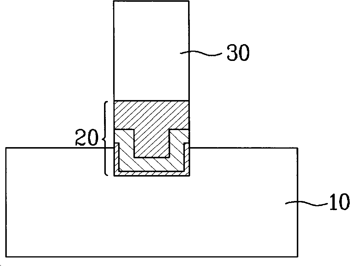
[0036] In particular, the present invention breaks away from the planar structure of the usual S...
PUM
 Abstract
Description
Claims
Application Information