1.5t dynamic memory cell, array and operation method based on resistive switching gate dielectric

A technology of dynamic storage and cell array, applied in the field of memory, can solve problems such as poor compatibility of CMOS process

Inactive Publication Date: 2016-08-03
FUDAN UNIV
View PDF3 Cites 0 Cited by
  • Summary
  • Abstract
  • Description
  • Claims
  • Application Information

AI Technical Summary

Problems solved by technology

[0003] The purpose of the present invention is to solve the difficulty of traditional 1T1CDRAM unit scalingdown, and the problem of poor compatibility with standard CMOS technology, in view of this, the present invention provides a kind of 90nm and following node dynamic memory (especially embedded memory) A solution especially compatible with standard logic's CMOSHfOxhighkmetalgate technology

Method used


Image

  • 1.5t dynamic memory cell, array and operation method based on resistive switching gate dielectric
  • 1.5t dynamic memory cell, array and operation method based on resistive switching gate dielectric
  • 1.5t dynamic memory cell, array and operation method based on resistive switching gate dielectric

Examples


Embodiment Construction

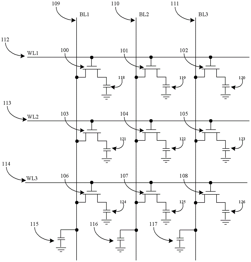
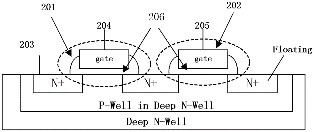
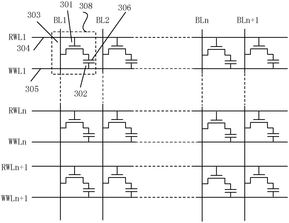
[0020] According to an embodiment of the present invention, the 1.5T dynamic memory cell and the array based on the resistive gate dielectric include: a transistor, including a source, a drain, and a control gate; a storage node, that is, the gate dielectric of the transistor control gate, located at the Between the control gate and the silicon substrate, the storage resistance changes; the word line is connected to the control gate of the transistor; the bit line is connected to the drain of the transistor; the source line is connected to the source of the transistor . Reference attached figure 2 , is a 1.5T dynamic memory cell based on a resistive gate medium according to an embodiment of the present invention, wherein 201 is named as a read tube, which plays the role of gating and current limiting, 202 is a programming component, 203 is a bit line, and 204 represents The word line 201 is the read word line, and 205 represents the programming word line. The gate 206 is ma...


PUM


Abstract

The invention relates to the technical field of memories and relates to a 1.5T dynamic memory unit and array structure based on a resistance variation gate dielectric and a method for operating the same. The 1.5T dynamic memory unit and array structure comprises a transistor, a memory node, a word line, a bit line and a source line, wherein the transistor comprises a source electrode, a drain electrode and a control gate electrode; the memory node is the gate dielectric of the control gate electrode of the transistor and is positioned between the control gate electrode of the transistor and a silicon substrate and used for storing resistance variation states; the word line is connected to the control gate electrode of the transistor; the bit line is connected to the drain electrode of the transistor; the source line is connected to the source electrode of the transistor; a read tube 201 has the effects of gating and limiting current, 202 is a programming part, 203 is the bit line, 204 is the word line of the 201, and 205 is a programming word line; the gate electrode has a high-resistance state and a low-resistance state; the conversion between the high-resistance state and the low-resistance state is reversible; and a certain voltage is applied between the bit line and the word line so as to generate different currents. According to the 1.5T dynamic memory unit and array structure, the problems of difficulty in scaling down and poorer compatibility with the standard CMOS process in a conventional 1T1C (1 Transistor and 1 Capacitor) DRAM (Dynamic Random Access Memory) unit are solved, and the 1.5T dynamic memory unit and array structure can be compatible with a standard logic CMOS HfOx high k metal gate technology.

Description

technical field [0001] The invention relates to the field of memory technology, in particular to a 1.5T dynamic memory unit based on a resistive variable gate medium, an array structure, and an operation method thereof. Background technique [0002] A storage cell of a traditional DRAM typically includes two elements, namely a storage capacitor and an access transistor, forming a 1T1C structure. See attached figure 1 , is a traditional DRAM array structure, where 100 to 108 are access transistors, 109 to 111 are bit lines, 112 to 114 are word lines, 115 to 117 are parasitic capacitances on bit lines, and 118 to 126 are storage capacitors . The working process of the traditional DRAM will be described below by taking the storage unit formed by operating the access transistor 100 and the storage capacitor 118 as an example. In the write operation phase, the data value is placed on the bit line 109, and the word line 112 is raised. According to the difference of the data val...

Claims


Application Information

Patent Timeline
Patent Type & Authority Patents(China)
IPC IPC(8): G11C11/406H01L27/108
Inventor 林殷茵李慧
Owner FUDAN UNIV
Why Eureka
Try Eureka