Semiconductor device

A technology of semiconductors and reading devices, applied in semiconductor devices, transistors, electric solid-state devices, etc., can solve problems such as data loss of storage units

Active Publication Date: 2020-10-20
WINBOND ELECTRONICS CORP
View PDF6 Cites 0 Cited by
  • Summary
  • Abstract
  • Description
  • Claims
  • Application Information

AI Technical Summary

Problems solved by technology

In order to increase the write margin, it is required to reduce the supply voltage Vdd provided to the memory cell, so that the current Id of the pull-up transistor becomes smaller; but on the other hand, this sometimes causes data loss of the memory cell

Method used


Image

  • Semiconductor device
  • Semiconductor device
  • Semiconductor device

Examples


Embodiment Construction

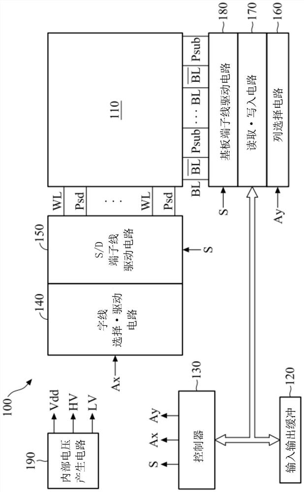
[0060] Next, examples of the present invention will be described. figure 2 Shows the configuration of the SRAM related to the embodiment of the present invention. As shown in the figure, SRAM 100 includes: memory cell array 110, which is configured by rows and columns of memory cells; input and output buffer 120, maintaining address or data; controller 130, controlling read operation or write operation, etc.; word line selection. The drive circuit 140 drives the selected word line corresponding to the decoding result of the row address Ax; the S / D terminal line drive circuit 150 drives the selected word line connected to the S / D terminal of the pull-up transistor corresponding to the decoding result of the row address Ax. S / D terminal line; the column selection circuit 160, corresponding to the decoding result of the column address Ay, selects the bit line BL, The read / write circuit 170 reads the data held in the memory cell through the selected pair of bit lines, and writes...


PUM


Abstract

A semiconductor device is provided. An SRAM of the invention includes P-well regions PW_1 and PW_2, an N-well region NW, a first metal wire M1, and a second metal wire M2. The P-well regions PW_1 andPW_2 extend in a first direction, and pull-down transistors and accessing transistors are formed therein. The N-well region NW extends in first direction, and pull-up transistors are formed therein. The first metal wire M1 extends in the first direction on the N-well region NW and is electrically connected to the N-well region NW. The second metal wire M2 extends in a second direction orthogonal to the first direction and electrically connected to a common S / D region of a pair of pull-up transistors that are formed in the N-well region NW. The semiconductor can apply different voltages to sources and bases of pull-up transistors and improves write margin of memory cells.

Description

technical field [0001] The present invention relates to a Static Random Access Memory (SRAM, Static Random Access Memory), in particular to a layout of memory cells for improving write margin (Margin). Background technique [0002] As a high-speed memory capable of random reading and writing, SRAM is widely used in cache memory and the like. Generally, a memory cell of an SRAM is composed of a pair of access transistors (pass gate transistors) and a latch circuit that is coupled to a pair of CMOS inverters. [0003] The writing margin of the SRAM is determined by the ratio of the drain current Id of the P-type pull-up transistor and the N-type channel gate transistor, which is also called the Gamma Ratio. In order to increase the write margin, it is required to reduce the supply voltage Vdd provided to the memory cell, so that the current Id of the pull-up transistor becomes smaller; but on the other hand, this sometimes causes data loss of the memory cell. In order to avo...

Claims


Application Information

Patent Timeline
Patent Type & Authority Applications(China)
IPC IPC(8): G11C11/419G11C11/412
CPCG11C11/419G11C11/412G11C5/146H01L27/0207H10B10/12H10B10/18G11C5/025G11C5/06
Inventor 广津寿一伊藤大贵
Owner WINBOND ELECTRONICS CORP
Why Eureka
Try Eureka