Semiconductor device and electronic device

a technology of semiconductors and electronic devices, applied in the direction of electronic switching, power consumption reduction, pulse technique, etc., can solve the problem of insufficient data retention characteristics, and achieve the effect of excellent data retention characteristics and novel structur

Active Publication Date: 2016-12-13
SEMICON ENERGY LAB CO LTD
View PDF132 Cites 0 Cited by
  • Summary
  • Abstract
  • Description
  • Claims
  • Application Information

AI Technical Summary

Benefits of technology

[0009]Another object of one embodiment of the present invention is to provide a semiconductor device or the like that has a novel structure and excellent data retention characteristics. Another object of one embodiment of the present invention is to provide a semiconductor device or the like having a novel structure in which a potential applied to a back gate of a transistor can be constant.
[0019]According to one embodiment of the present invention, a semiconductor device or the like that has a novel structure and excellent data retention characteristics can be provided. According to one embodiment of the present invention, a semiconductor device or the like having a novel structure in which a potential applied to a back gate of a transistor can be constant can be provided.

Problems solved by technology

Accordingly, the potential applied to the back gate of a transistor fails to be constant, which might lead to insufficient data retention characteristics.

Method used


Image

  • Semiconductor device and electronic device
  • Semiconductor device and electronic device
  • Semiconductor device and electronic device

Examples


embodiment 1

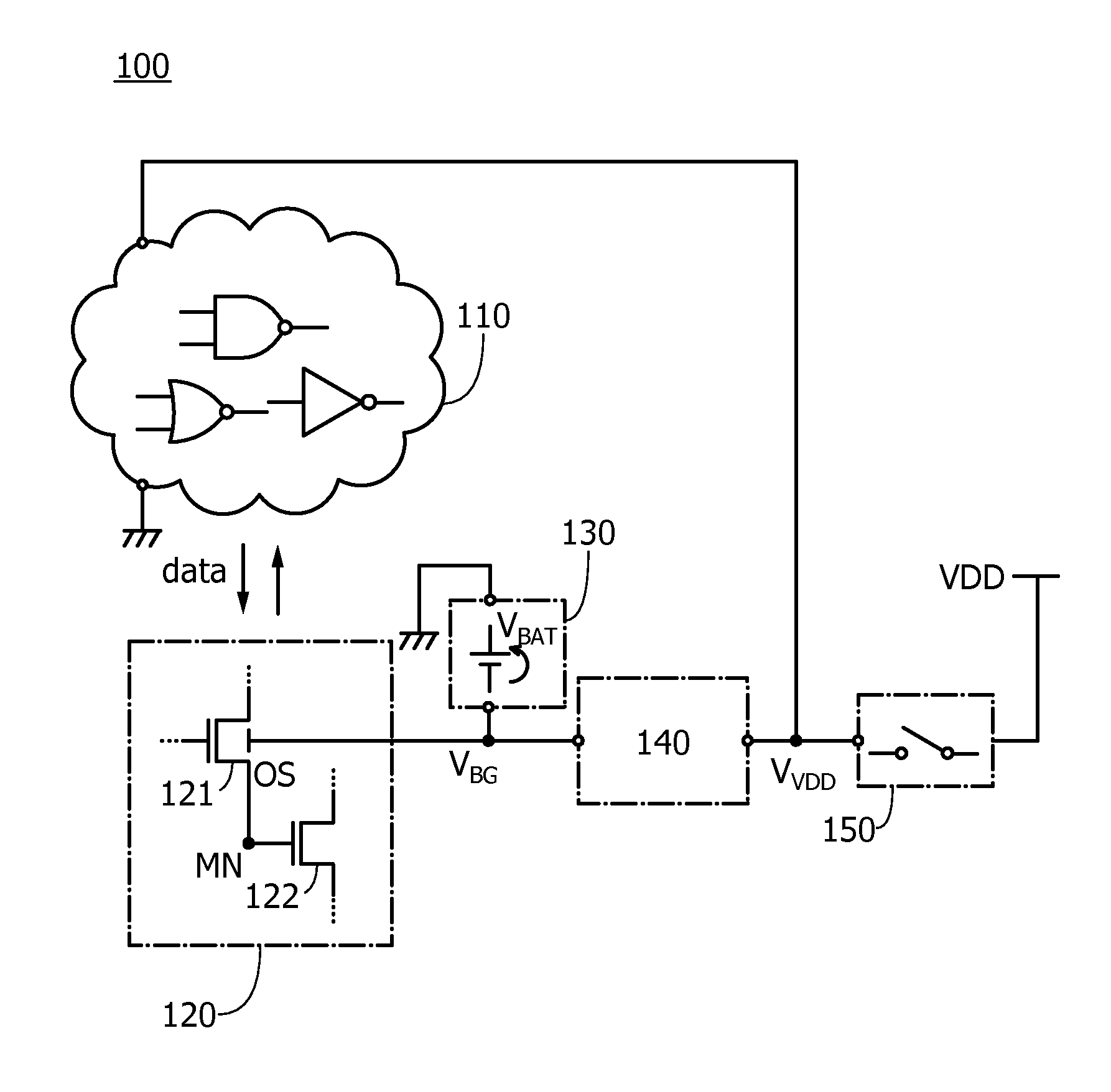
[0059]A configuration of a semiconductor device of one embodiment of the present invention is described with reference to FIG. 1.

[0060]In this specification and the like, the term “semiconductor device” refers to all devices that can operate by utilizing semiconductor characteristics. Furthermore, the term “semiconductor device” refers to a circuit utilizing semiconductor characteristics or the whole of a system that includes the circuit.

[0061]FIG. 1 is a block diagram showing the configuration of a semiconductor device of one embodiment of the present invention.

[0062]In FIG. 1, a semiconductor device 100 includes a circuit 110, a circuit 120, a battery 130, a voltage generation circuit 140, and a switch 150. The circuit 120 includes a transistor 121 and a transistor 122.

[0063]In one embodiment of the present invention, the transistor 121 with a low off-state current in the circuit 120 is utilized to save and retain data stored in the circuit 110, and a potential to be applied to a ...

embodiment 2

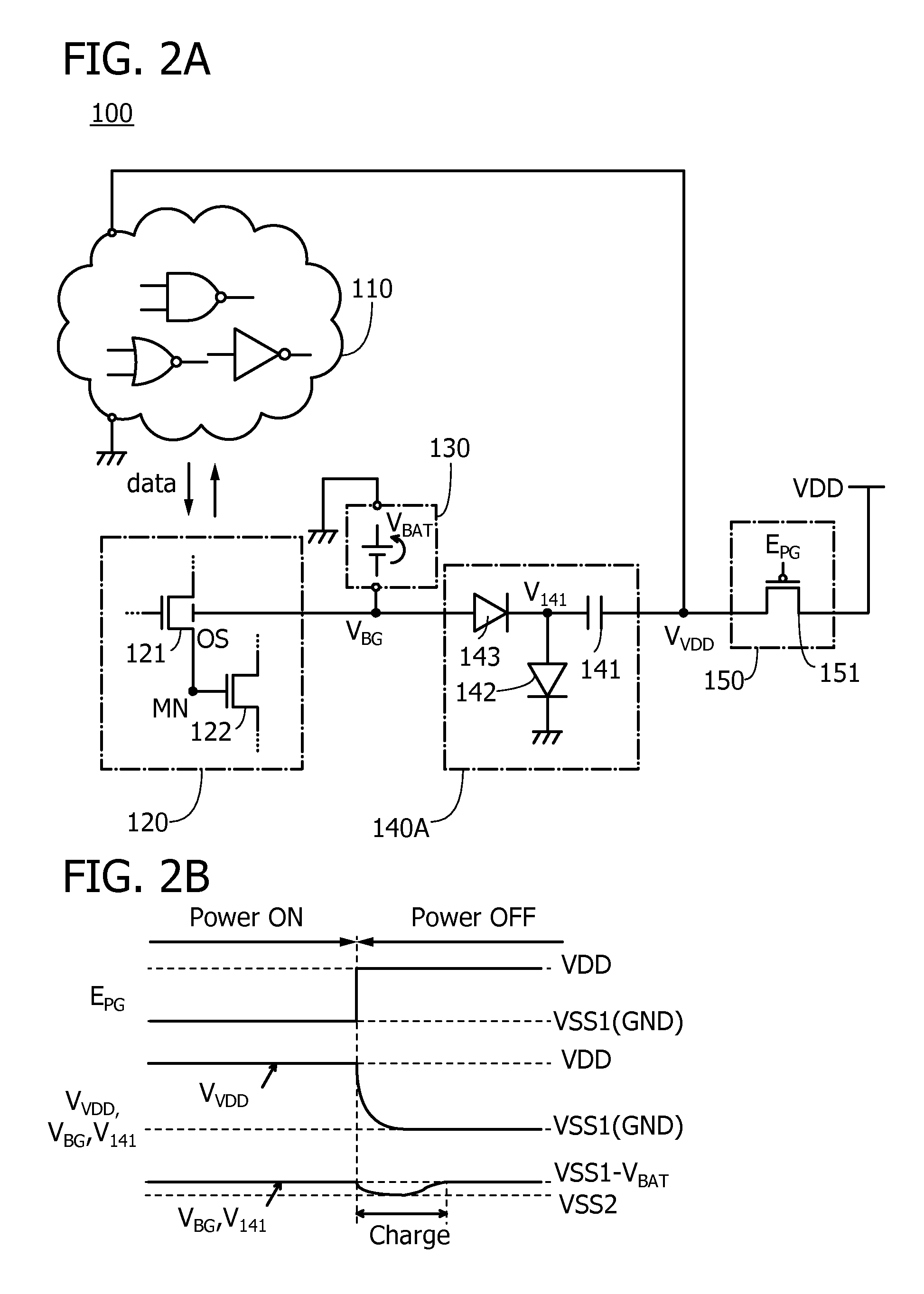
[0108]In this embodiment, an example of a circuit configuration different from that described in Embodiment 1 is described. In particular, a circuit configuration and an operation that are different from those of the voltage generation circuit in Embodiment 1 are described in this embodiment.

[0109]In a circuit diagram of the semiconductor device 100 in FIG. 3, a voltage generation circuit 140B includes an oscillator circuit 144 in addition to the capacitor 141 and the diodes 142 and 143. The oscillator circuit 144 includes an inverter chain of inverters 145 and a NOR 146 to which a control signal EN and an output signal of the oscillator circuit 144 are input.

[0110]A power supply voltage is supplied to the inverters 145 and the NOR 146 when the potential VVDD changes to the potential VDD. In the oscillator circuit 144, oscillation is controlled in accordance with the control signal EN. In FIG. 3, the potential of the output signal of the oscillator circuit 144 is referred to as a po...

embodiment 3

[0119]In this embodiment, examples of the circuit 110 and the circuit 120 described in Embodiment 1 or 2 and an operation thereof are described. FIG. 6A illustrates a specific circuit diagram of the circuits 110 and 120. The circuits 110 and 120 illustrated as an example in FIG. 6A are function as a latch circuit 200 capable of saving data. Data is retained in the circuit 110 during supply of a power supply voltage, whereas the data is retained in the circuit 120 when the supply of a power supply voltage is stopped.

[0120]The circuit 110 includes a node N1 and a node N2, at which potentials corresponding to data “1” and data “0” can be held during the period of continuing the supply of a power supply voltage. The potential VVDD and the potential VSS1, which are described in Embodiment 1, are applied to the circuit 110.

[0121]The circuit 110 includes, for example, an inverter 101, an inverter 102, a switch 103, an inverter 104, and a switch 105.

[0122]For example, a data signal D, a clo...


PUM


Abstract

A semiconductor device having excellent data retention characteristics. A transistor with a low off-state current is utilized to save and retain data stored in a memory circuit, and a potential to be applied to a back gate of the transistor is applied from a battery provided for each memory circuit. The potential applied to the back gate of the transistor and a potential for charging the battery are generated in a voltage generation circuit. The battery is charged utilizing power gating of the memory circuit and data retention characteristics is improved.

Description

BACKGROUND OF THE INVENTION[0001]1. Field of the Invention[0002]One embodiment of the present invention relates to a semiconductor device and an electronic device.[0003]Note that one embodiment of the present invention is not limited to the above technical field. The technical field of the invention disclosed in this specification and the like relates to an object, a method, or a manufacturing method. In addition, one embodiment of the present invention relates to a process, a machine, manufacture, or a composition of matter. Specifically, examples of the technical field of one embodiment of the present invention disclosed in this specification include a semiconductor device, a display device, a light-emitting device, a power storage device, an imaging device, a memory device, a method for driving any of them, and a method for manufacturing any of them.[0004]2. Description of the Related Art[0005]Patent Document 1 discloses a configuration in which a potential for controlling a thre...

Claims


Application Information

Patent Timeline
Patent Type & Authority Patents(United States)
IPC IPC(8): H03K17/687H01L23/58H01L21/8258H03K19/00H01L27/06
CPCH01L21/8258H01L23/58H03K17/687H01L27/0688H03K19/0013H03K2217/0027H01L2924/0002H01L27/1225H01L2924/00H01L29/7869
Inventor KUROKAWA, YOSHIYUKIIKEDA, TAKAYUKI
Owner SEMICON ENERGY LAB CO LTD
Why Eureka
Try Eureka