Lateral trench field-effect transistors in wide bandgap semiconductor materials, methods of making

A field effect transistor, semiconductor technology, applied in transistors, semiconductor devices, thyristors, etc., can solve problems such as threshold voltage drift, difficulty in achieving monolithic integration, and low reverse channel mobility

Inactive Publication Date: 2008-12-03
PI
View PDF12 Cites 6 Cited by
  • Summary
  • Abstract
  • Description
  • Claims
  • Application Information

AI Technical Summary

Problems solved by technology

Other issues include: low reverse channel mobility due to high interface state density at the SiC/SiO2 interface and high fixed charge density in the insulator; and Threshold voltage drifts sign

Method used


Image

  • Lateral trench field-effect transistors in wide bandgap semiconductor materials, methods of making
  • Lateral trench field-effect transistors in wide bandgap semiconductor materials, methods of making
  • Lateral trench field-effect transistors in wide bandgap semiconductor materials, methods of making

Examples


Embodiment Construction

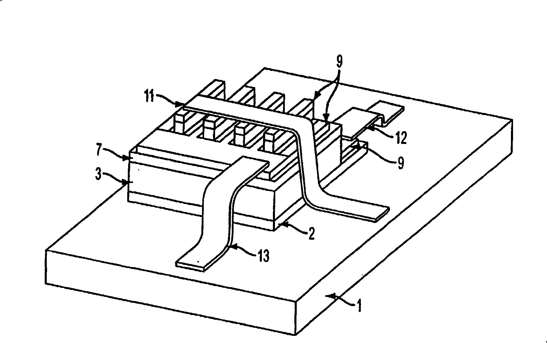
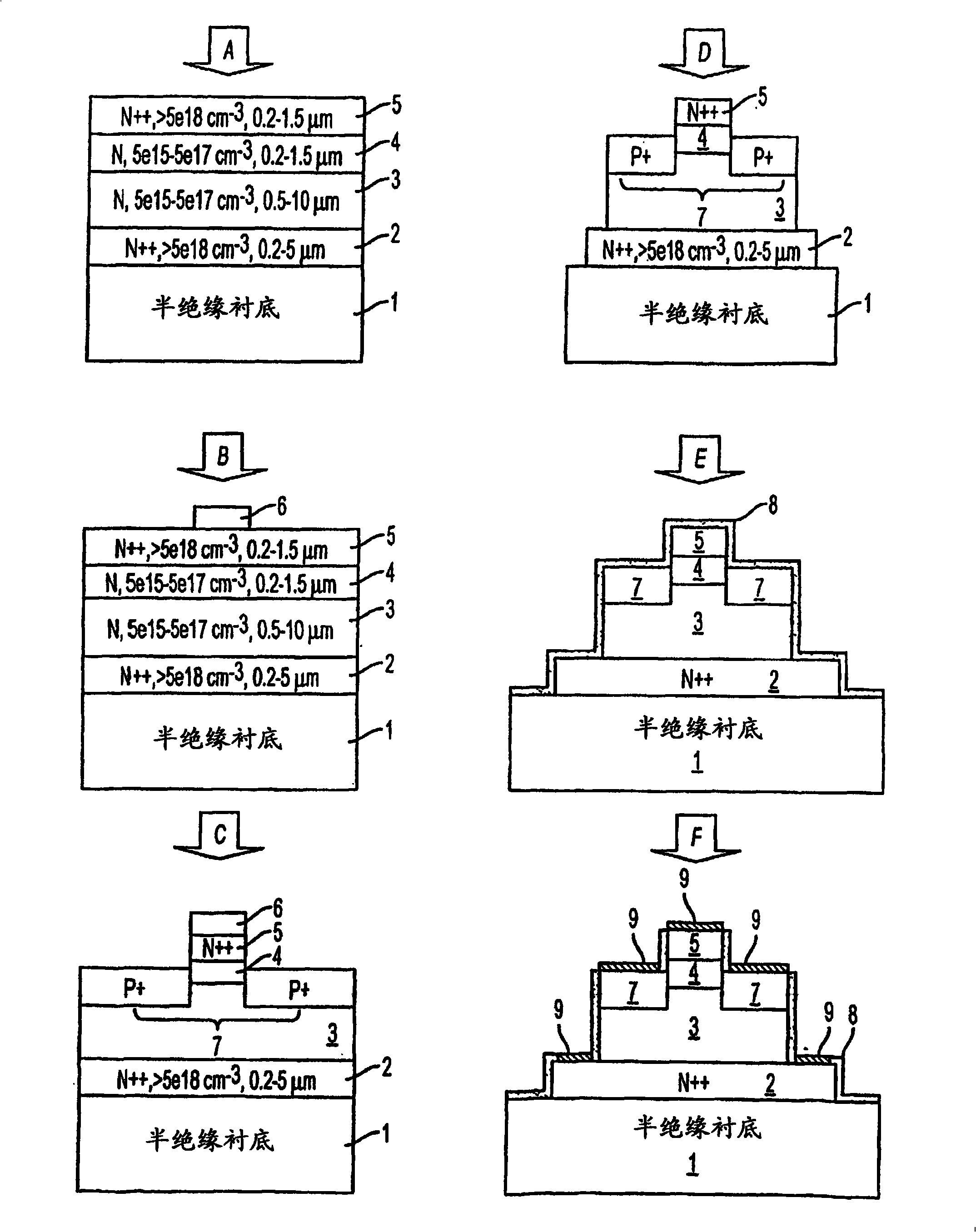
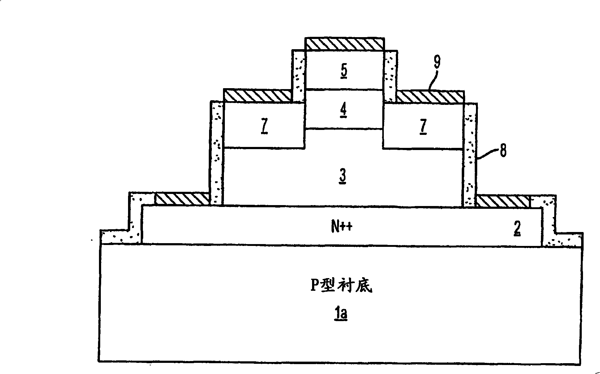
[0079] Provides a vertical channel junction field effect transistor (JFET) that can be electrically isolated from other devices fabricated on the same die and that can be made in such a way that devices fabricated on the same die have different threshold voltages to fulfill. Also provided are monolithic integrated circuits comprising the devices described above and methods of making the devices and integrated circuits comprising the devices.

[0080] The present invention generally relates to junction field effect transistors (JFETs) having vertical channels and monolithic integrated circuits fabricated using such devices. In particular, the invention relates to such transistors and circuits formed in wide bandgap semiconductor materials.

[0081] The device can be built in a wide bandgap (i.e. E G >2eV) semiconductor substrate, the substrate can be a semi-insulating, p-type substrate or an n-type substrate with a p-type buffer layer. The device may include source, channel,...


PUM


Abstract

A junction field effect transistor is described. The transistor is made from a wide bandgap semiconductor material. The device comprise source, channel, drift and drain semiconductor layers, as well as p-type implanted or Schottky gate regions. The source, channel, drift and drain layers can be epitaxially grown. The ohmic contacts to the source, gate, and drain regions can be formed on the same side of the wafer. The devices can have different threshold voltages depending on the vertical channel width and can be implemented for both depletion and enhanced modes of operation for the same channel doping. The devices can be used for digital, analog, and monolithic microwave integrated circuits. Methods for making the transistors and integrated circuits comprising the devices are also described.

Description

[0001] This application is related to U.S. Patent Application 60 / 585,881 filed on July 8, 2004 and the application entitled "Normally-Off Integrated JFET PowerSwitches in Wide Bandgap Semiconductors and Methods of Making" filed on December 1, 2004. normally-off integrated JFET power switch and method of manufacture)" in US Patent Application 11 / 000,222. Each of the above applications is fully incorporated herein by reference. technical field [0002] This invention relates generally to lateral field effect transistors (FETs) having vertical channels, and in particular to such transistors formed in wide bandgap semiconductor materials. The invention also relates to monolithic integrated circuits comprising such transistors. Background technique [0003] Wide bandgap semiconductor materials (E G >2eV) such as silicon carbide (SiC) or Group III nitride compound semiconductors (eg gallium nitride GaN) are very attractive for use in high power, high temperature and / or radiat...

Claims


Application Information

Patent Timeline
IPC IPC(8): H01L29/74H01L29/423H01L31/111
CPCH01L29/2003H01L27/098H01L29/1608H01L29/808H01L29/47H01L29/8122H01L29/80
Inventor 伊格尔·桑金杰弗里·B.·卡萨德约瑟夫·N.·梅里特
Owner PI
Why Eureka
Try Eureka