ROM structure and method for writing in INTEL HEX file
A file and architecture technology, applied in the field of ROM structure, can solve the problem of not being able to provide enough memory data for the host of the single-chip microcomputer, reducing the working efficiency of the single-chip microcomputer of the RISC system, etc., to achieve the effect of reducing resources
- Summary
- Abstract
- Description
- Claims
- Application Information
AI Technical Summary
Problems solved by technology
Method used
Image
Examples
Embodiment Construction
[0023] 1. The structure of ROM
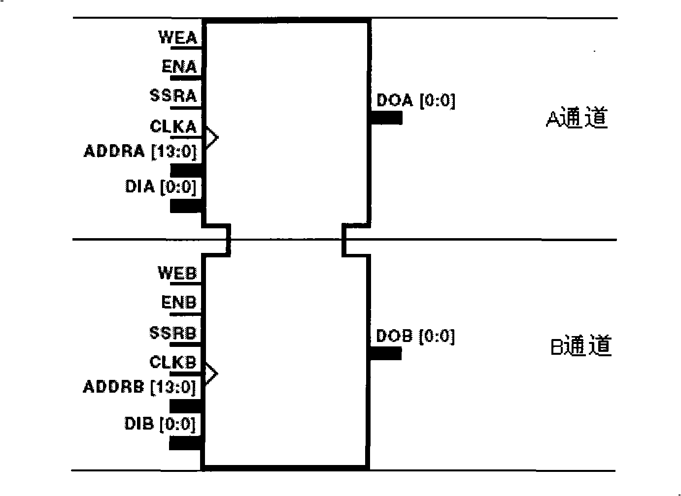
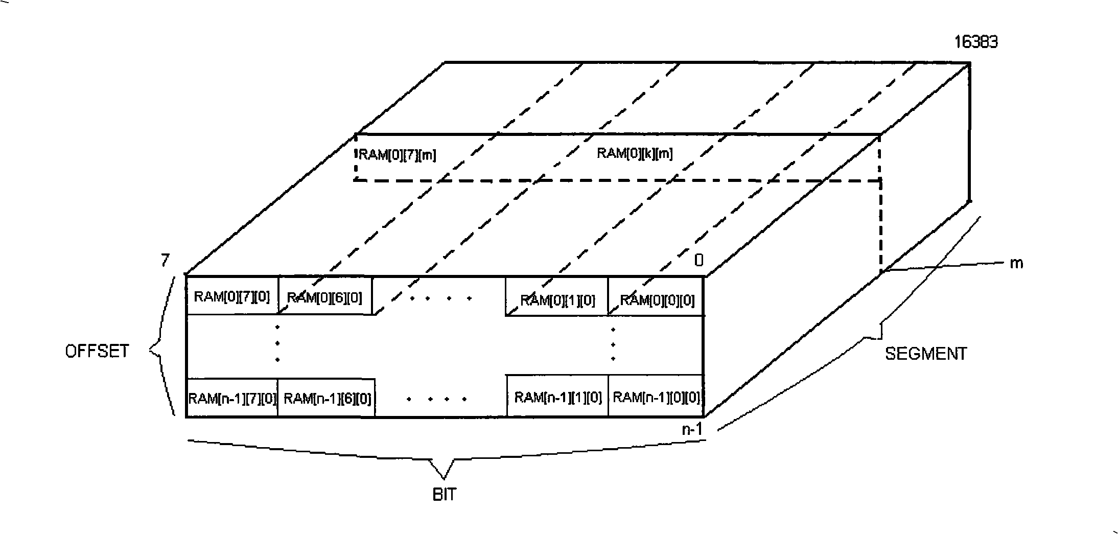
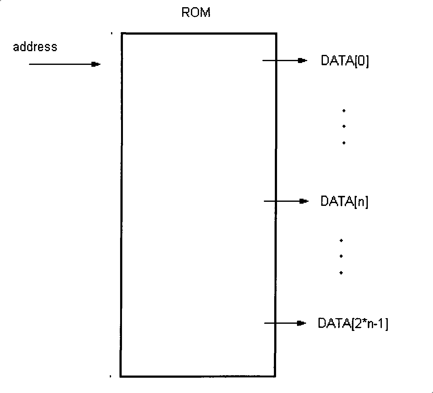
[0024] Dual-channel RAM is integrated in the FPGA chip, which can be combined into ROM. In the embodiment of the present invention, the dual-channel RAM module inside the FPGA is used to form a ROM with single address input and multiple data output, that is, when the ROM is read, an address signal is input and multiple continuous data are output.
[0025] Existing dual-channel RAM modules such as figure 1 display, including A and B channels. Among them, WEA and WEB are the write signals of the two channels of the input RAM respectively. ENA and ENB are respectively the enable signals of the two channels of the input RAM. SSRA and SSRB are respectively the reset signals of the two channels of the input RAM. CLKA and CLKB are the clock signals of the two channels of the input RAM respectively. ADDRA and ADDRB are the address signals of the two channels of the input RAM respectively. DIA and DIB are the data signals of the two channels of th...
PUM
 Abstract
Description
Claims
Application Information


