Apparatus for heat treatment of wafer

A heat treatment device and wafer technology, applied in gaseous chemical plating, coating, electrical components, etc., can solve problems such as yield drop, long time, damage, etc., to reduce air residue, increase exhaust volume, and improve exhaust The effect of gas velocity

Inactive Publication Date: 2008-12-24
SEMICON MFG INT (SHANGHAI) CORP
View PDF1 Cites 1 Cited by
  • Summary
  • Abstract
  • Description
  • Claims
  • Application Information

AI Technical Summary

Problems solved by technology

[0010] However, when using the wafer heat treatment device to work, it takes a long time to exhaust the air in the loading chamber 208 through the exhaust pipe 272, and there is air remaining at the end of the wafer boat 261 near the opening 241a; The air residue is brought into the liner 241 when the crystal boat 261 rises, and the oxygen in the air residue will affect the heat treatment of the semiconductor wafer; It will cause damage to the devices on the semiconductor wafer and reduce the yield

Method used


Image

  • Apparatus for heat treatment of wafer
  • Apparatus for heat treatment of wafer
  • Apparatus for heat treatment of wafer

Examples


Embodiment Construction

[0032] The specific embodiments of the present invention will be described in detail below in conjunction with the accompanying drawings.

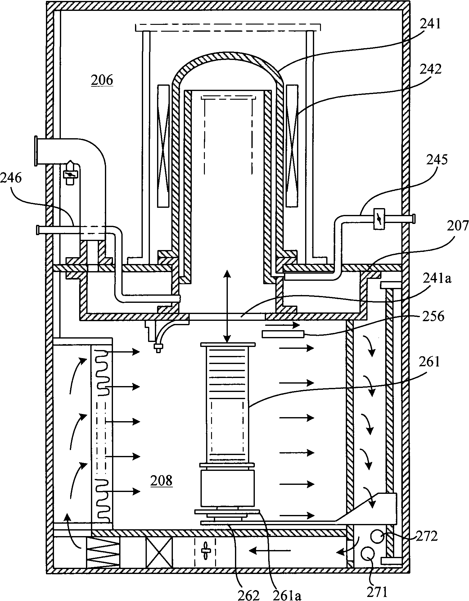
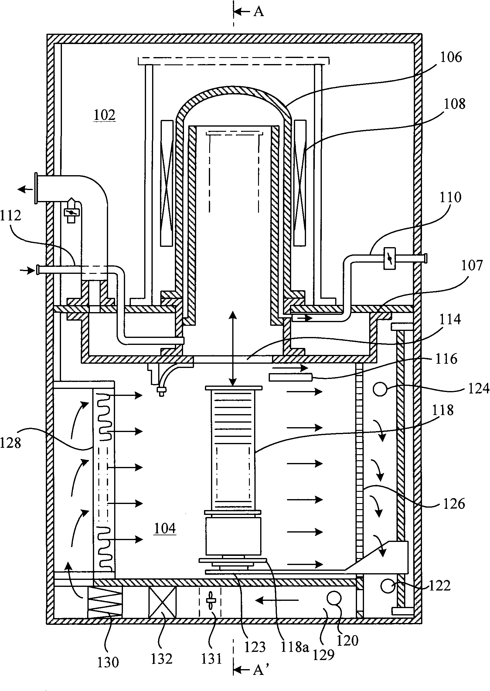
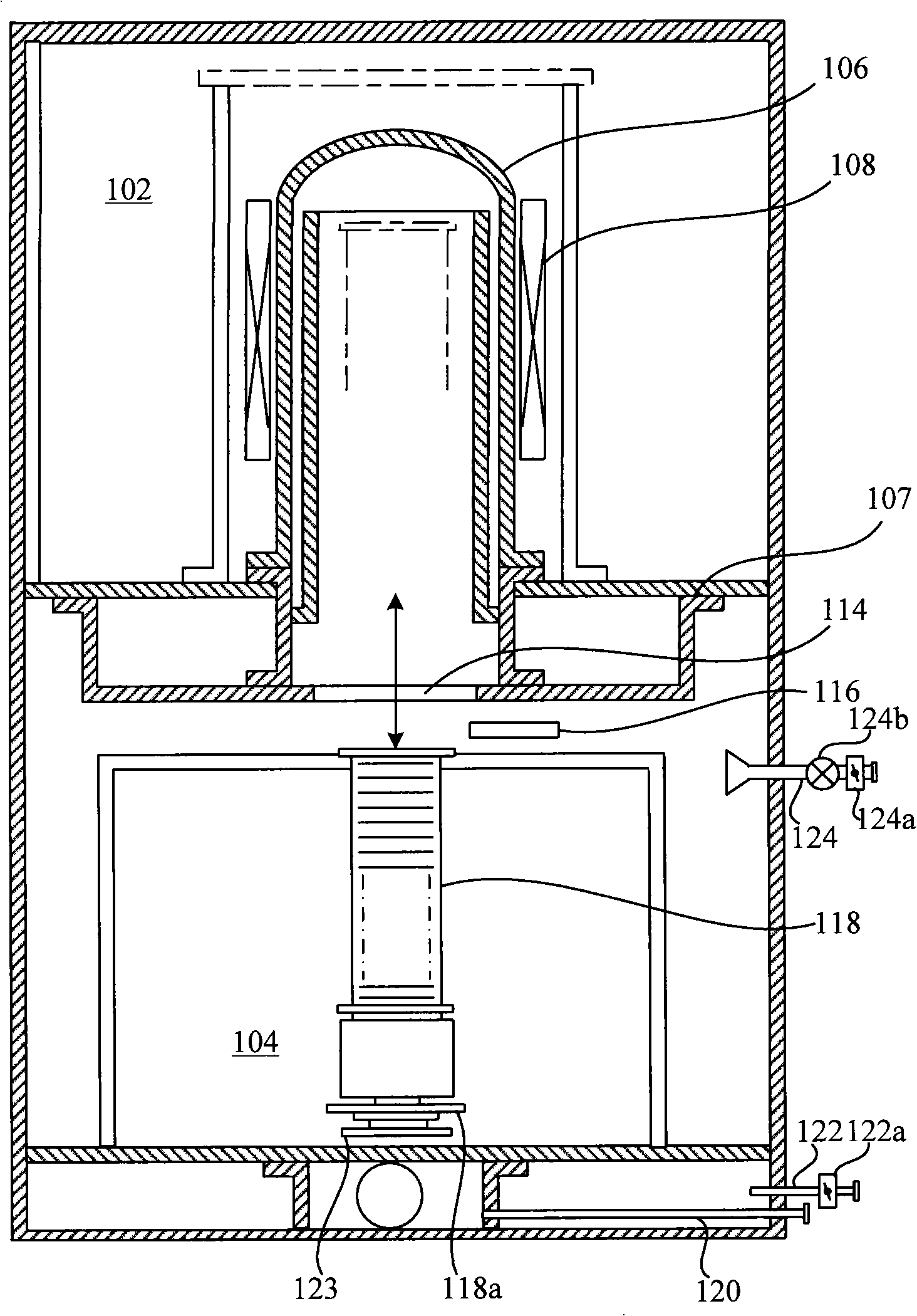
[0033] figure 2 It is a schematic cross-sectional view of the first embodiment of the wafer heat treatment device of the present invention, image 3 for figure 2 Schematic cross-section along AA'. Such as figure 2 As shown, the loading chamber 104 is located below the heat treatment process chamber 102 , and the spacer 107 is hermetically sealed between the loading chamber 104 and the heat treatment process chamber 102 .

[0034] There is a vertically placed liner 106 in the heat treatment process chamber 102. The liner 106 is an inverted "U" shape with a closed upper end and a lower end connected to the isolation device 107. The liner 106 is made of quartz. Multiple sets of heaters 108 are distributed on the sidewall of the liner 106; the heaters 108 may be resistance wires. The heater 108 heat-treats the semiconductor wafer in th...


PUM


Abstract

The invention relates to wafer heat treatment equipment which comprises a loading chamber and an air supply pipe. The air supply pipe is connected with the loading chamber to supply the loading chamber for air; the wafer heat treatment equipment also comprises at least two exhaust pipes connected with the loading chamber, which exhausts air in the loading chamber. The air exhaust speed of the wafer heat treatment equipment is quicker and comparatively little air is left.

Description

technical field [0001] The invention relates to the technical field of semiconductor manufacturing, in particular to a wafer heat treatment device in a semiconductor manufacturing process. Background technique [0002] In the semiconductor manufacturing process, the wafer heat treatment device is used to grow film layers on the surface of the semiconductor wafer or perform thermal annealing treatment on the semiconductor wafer. At present, a vertical wafer heat treatment device is commonly used. US Patent No. US 5562383 discloses a wafer heat treatment device. figure 1 It is a schematic cross-sectional view of the wafer heat treatment device disclosed in the US patent. [0003] Such as figure 1 As shown, the wafer heat treatment apparatus includes a heat treatment process chamber 206, a loading chamber 208 located below the heat treatment process chamber 206, and an isolation device 207 between the heat treatment process chamber 206 and the loading chamber 208; [0004] ...

Claims


Application Information

Patent Timeline
IPC IPC(8): H01L21/00H01L21/205H01L21/324H01L21/67C23C16/44
Inventor 赵星宋大伟李修远
Owner SEMICON MFG INT (SHANGHAI) CORP
Why Eureka
Try Eureka