Method for determining groove etch time and method for preparing isolation of shallow channel

A technology of etching time and manufacturing method, which is applied in semiconductor/solid-state device manufacturing, electrical components, circuits, etc., can solve the problems of difficult trench etching time and complicated process, and achieve simplification of research and development process, cost reduction, The effect of saving R&D costs

Active Publication Date: 2008-12-24
SEMICON MFG INT (SHANGHAI) CORP +1
View PDF1 Cites 4 Cited by
  • Summary
  • Abstract
  • Description
  • Claims
  • Application Information

AI Technical Summary

Problems solved by technology

[0009] In the manufacturing method of the shallow trench isolation, the semiconductor substrate 12 at the bottom of the opening 16C is etched, and the semiconductor substrate 12 is formed in the semiconductor substrate 12 such as image 3 The method of the trench 18 shown is generally plasma dry etching. Since there is no etch stop layer during the etching process, the depth of the trench 18 needs to be controlled by the etching time; In the case of a certain etching material, the etching time of the groove is also affected by the density of the groove. For the same depth of the groove, the etching time is different due to the different density; therefore, in order to obtain a depth satisfying The etching time of the groove required requires a large number of experiments, making it difficult to determine the etching time of the groove; especially in the development of new products, in order to obtain the shallow trench isolation in the manufacturing process of the new product The etching time of the trench has to be carried out a large number of experiments, which complicates the process of developing this new product

Method used


Image

  • Method for determining groove etch time and method for preparing isolation of shallow channel
  • Method for determining groove etch time and method for preparing isolation of shallow channel
  • Method for determining groove etch time and method for preparing isolation of shallow channel

Examples


Embodiment Construction

[0051] The specific embodiments of the present invention will be described in detail below in conjunction with the accompanying drawings.

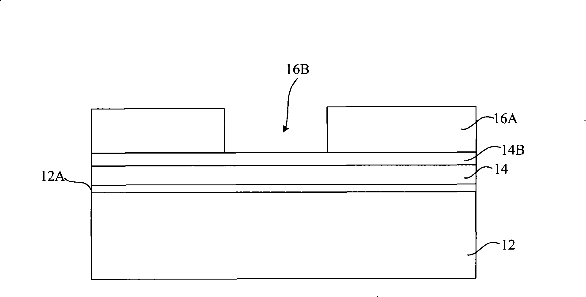
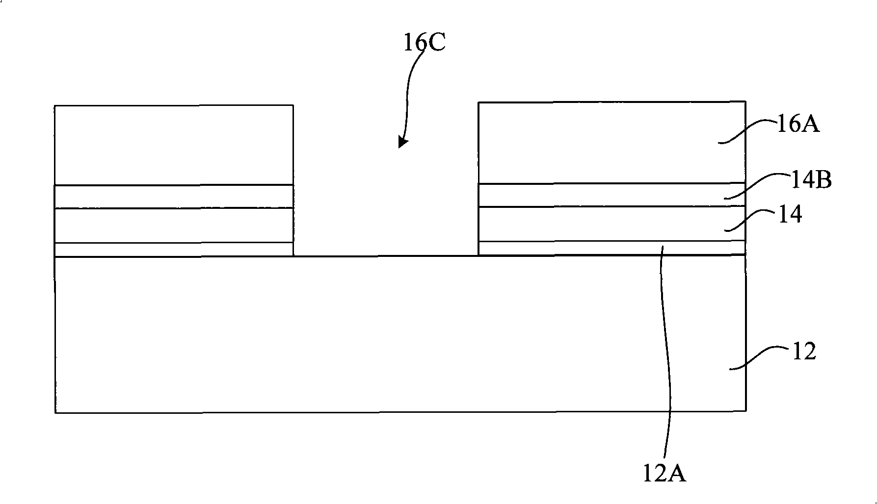
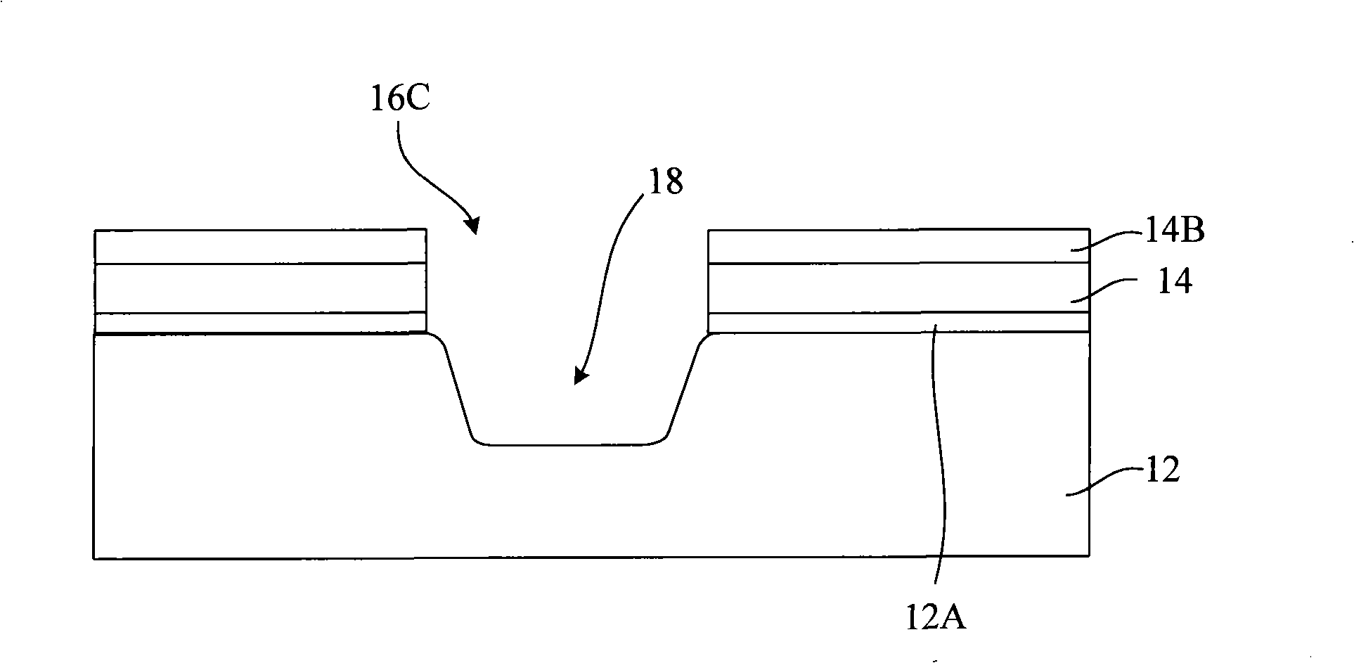
[0052] In the semiconductor manufacturing process, it is often necessary to make trenches in the semiconductor substrate, for example, when forming an active region, it is necessary to form an isolation trench in the semiconductor substrate; when etching the trench in the semiconductor substrate, the etching time It is not only related to the depth of the trench, but also related to the density of the trench. The etching time of trenches with different densities is different; and with the development of semiconductor manufacturing processes, the integration level is getting higher and higher. The density of grooves in different products is not the same, and the etching time of grooves needs to be determined through more experiments and tests, which brings great difficulties to the determination of groove etching conditions; for For the det...


PUM


Abstract

The invention relates to a method for determining the etching time of a plow groove, which comprises the steps as follows: a first mask which has a plow groove design is provided and the light transmission ratio of the first mask is obtained; the value of the light transmission ratio is input into the functional relationship of the light transmission ratio of a second mask which is obtained beforehand, and the etching time of the plow groove to calculate the etching time of the plow groove which is corresponding to the plow groove design of the first mask, wherein, the second mask is provided with the plow groove design and the plow groove design of the second mask and the plow groove design of the first mask have the same technology nodes. The invention also provides a manufacturing method for the isolation of a shallow plow groove. The technique for obtaining the etching time of the plow groove of the invention is relatively simple and can save time.

Description

technical field [0001] The invention relates to the technical field of semiconductor manufacturing, in particular to a method for determining trench etching time and a manufacturing method for shallow trench isolation. Background technique [0002] In the manufacturing process of semiconductor integrated circuits, shallow trench isolation is formed by forming a trench on a semiconductor substrate and then filling the trench with a dielectric material. The Chinese patent application document with publication number CN1649122A (published on August 3, 2005) discloses a manufacturing method for shallow trench isolation. [0003] Figure 1 to Figure 5 A schematic cross-sectional view of a structure corresponding to each step of the shallow trench isolation manufacturing method disclosed in the Chinese patent application document. [0004] Such as figure 1 As shown, a semiconductor substrate 12 is provided, a pad oxide layer 12A is formed on the semiconductor substrate 12, and ...

Claims


Application Information

Patent Timeline
Patent Type & Authority Applications(China)
IPC IPC(8): H01L21/308H01L21/762
Inventor 陈海华黄怡张海洋张世谋
Owner SEMICON MFG INT (SHANGHAI) CORP
Why Eureka
Try Eureka