Liquid crystal display panel and liquid crystal display panel assembling method

A liquid crystal display panel and substrate technology, applied in nonlinear optics, instruments, optics, etc., can solve problems such as the gravity margin of spots displayed on the liquid crystal display panel

Inactive Publication Date: 2008-12-31
INNOCOM TECH SHENZHEN +1
View PDF0 Cites 34 Cited by
  • Summary
  • Abstract
  • Description
  • Claims
  • Application Information

AI Technical Summary

Problems solved by technology

[0013] In order to solve the problems in the prior art that the liquid crystal display panel produces display spots due to uneven gravity distribution and the gravity margin is small, it is necessary to provide a liquid crystal display panel with uniform gravity distribution and a large gravity margin range.
[0014] In addition, in o

Method used


Image

  • Liquid crystal display panel and liquid crystal display panel assembling method
  • Liquid crystal display panel and liquid crystal display panel assembling method
  • Liquid crystal display panel and liquid crystal display panel assembling method

Examples


Embodiment Construction

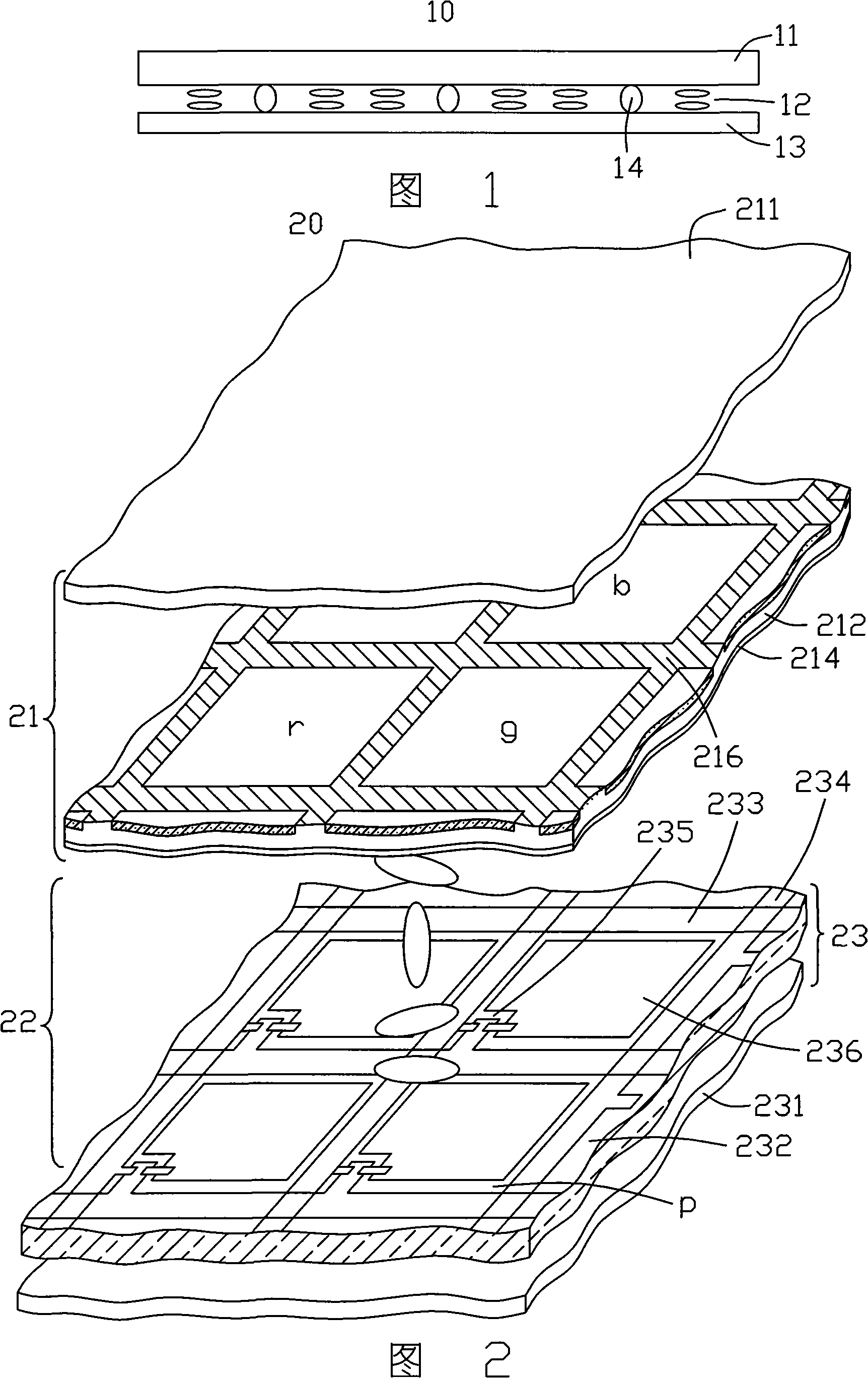
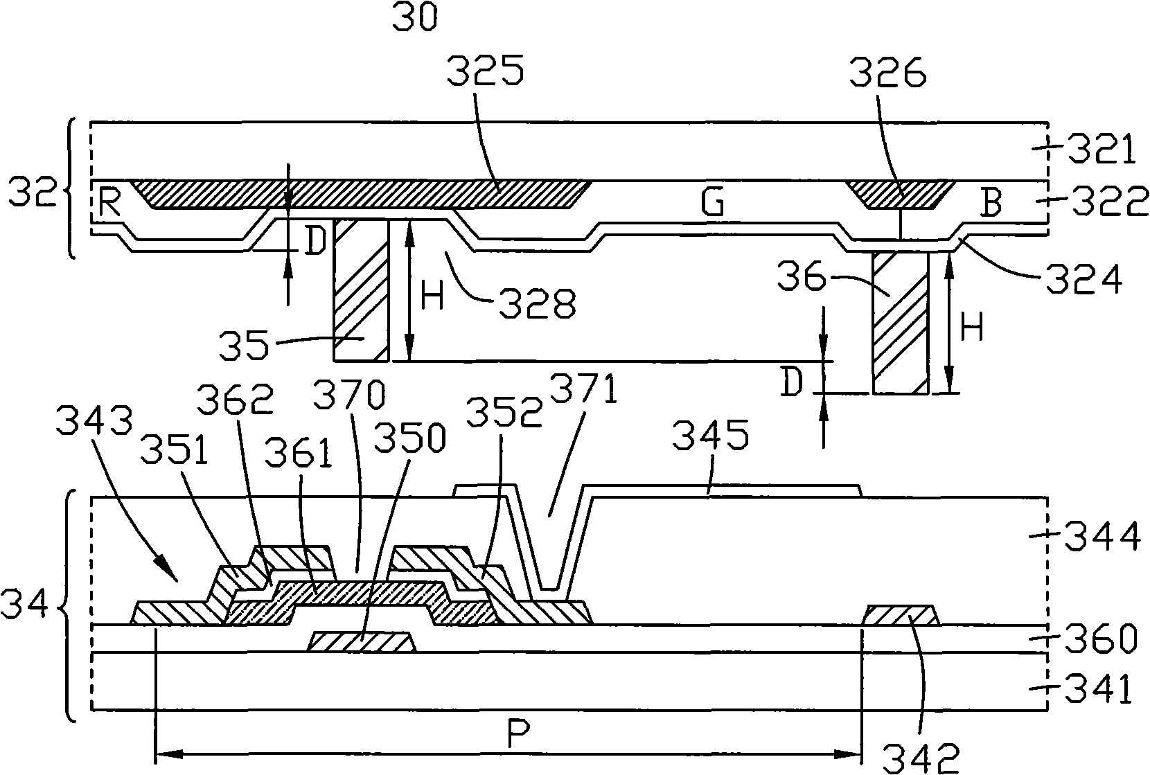
[0027] see Figure 4, is a schematic cross-sectional view of the first embodiment of the liquid crystal display panel of the present invention before assembly. The liquid crystal display panel 30 includes a color filter layer substrate 32 , a thin film transistor substrate 34 , a plurality of first columnar spacers 35 and a plurality of second columnar spacers 36 . The color filter substrate 32 is disposed opposite to the TFT substrate 34 , and the plurality of first columnar spacers 35 and the plurality of second columnar spacers 36 are located between the two substrates 32 , 34 .

[0028] The thin film transistor substrate 34 includes a first base 341 and a thin film transistor array (not shown) disposed on the surface of the first base 341 . The thin film transistor array includes a plurality of scanning lines arranged horizontally (not shown in the figure), a plurality of data lines 342 vertically insulated and intersecting with the scanning lines (only one of them is sho...


PUM


Abstract

The invention relates to a liquid crystal display panel and a liquid crystal display panel assembly method. The liquid crystal panel comprises a first substrate and a second substrate which is provided with a colourful filter layer. The colourful filter layer comprises a plurality of pixel units; each pixel unit comprises a first black matrix, a second black matrix which is arranged in an interval way to the first black matrix, a first cylindrical clearance article and a second cylindrical clearance article. The first cylindrical clearance article is arranged on the colourful filter layer correspondingly to the first black matrix. The second cylindrical clearance article is arranged on the colourful filter layer correspondingly to the second black matrix. The two cylindrical clearance articles, after being compressed, are respectively butted with the same horizontal surface of the first substrate and are used for supporting the two substrates; furthermore, the first cylindrical clearance article and the second cylindrical article are provided with different compression quantities. The liquid crystal display panel and the liquid crystal display panel assembly method can effectively avoid the display fleck problem caused by the non-uniform distribution of the gravity force and can obtain the gravity residues with large range.

Description

technical field [0001] The invention relates to a liquid crystal display panel and a method for assembling the liquid crystal display panel. Background technique [0002] Liquid crystal displays have been widely used in modern information equipment such as personal computers, mobile phones, and personal digital assistants due to their advantages of thinness, lightness, low power consumption, and low radiation. Generally, a liquid crystal display includes a liquid crystal display panel, a backlight module for providing planar light to the liquid crystal display panel, and a driving circuit for controlling the display of the liquid crystal display panel. [0003] Please refer to FIG. 1 , which is a schematic structural diagram of a liquid crystal display panel in the prior art. The liquid crystal display panel 10 includes a first substrate 11 , a liquid crystal layer 12 , a second substrate 13 and a plurality of spacers 14 . The first substrate 11 is opposite to the second s...

Claims


Application Information

Patent Timeline
IPC IPC(8): G02F1/1339G02F1/1333
Inventor 吴佳怡陈锡坚萧坤星
Owner INNOCOM TECH SHENZHEN
Why Eureka
Try Eureka