Check patentability & draft patents in minutes with Patsnap Eureka AI!

Manufacturing process of input/output device

A manufacturing method and device technology, applied in semiconductor/solid-state device manufacturing, electrical components, circuits, etc., can solve the problems of inability to obtain a graded junction, low temperature, etc., and achieve the effect of preventing hot carrier effects

Inactive Publication Date: 2008-12-31
SEMICON MFG INT (SHANGHAI) CORP
View PDF0 Cites 0 Cited by
  • Summary
  • Abstract
  • Description
  • Claims
  • Application Information

AI Technical Summary

Problems solved by technology

This thermal process can be effectively utilized if the N I / O ion implantation step is brought before the additional sidewall deposition step, however, the temperature of the additional sidewall deposition is only 650°C, which is too low to obtain the ideal graded junction , therefore, it is necessary to add an additional heat process

Method used


Image

  • Manufacturing process of input/output device
  • Manufacturing process of input/output device

Examples


Embodiment Construction

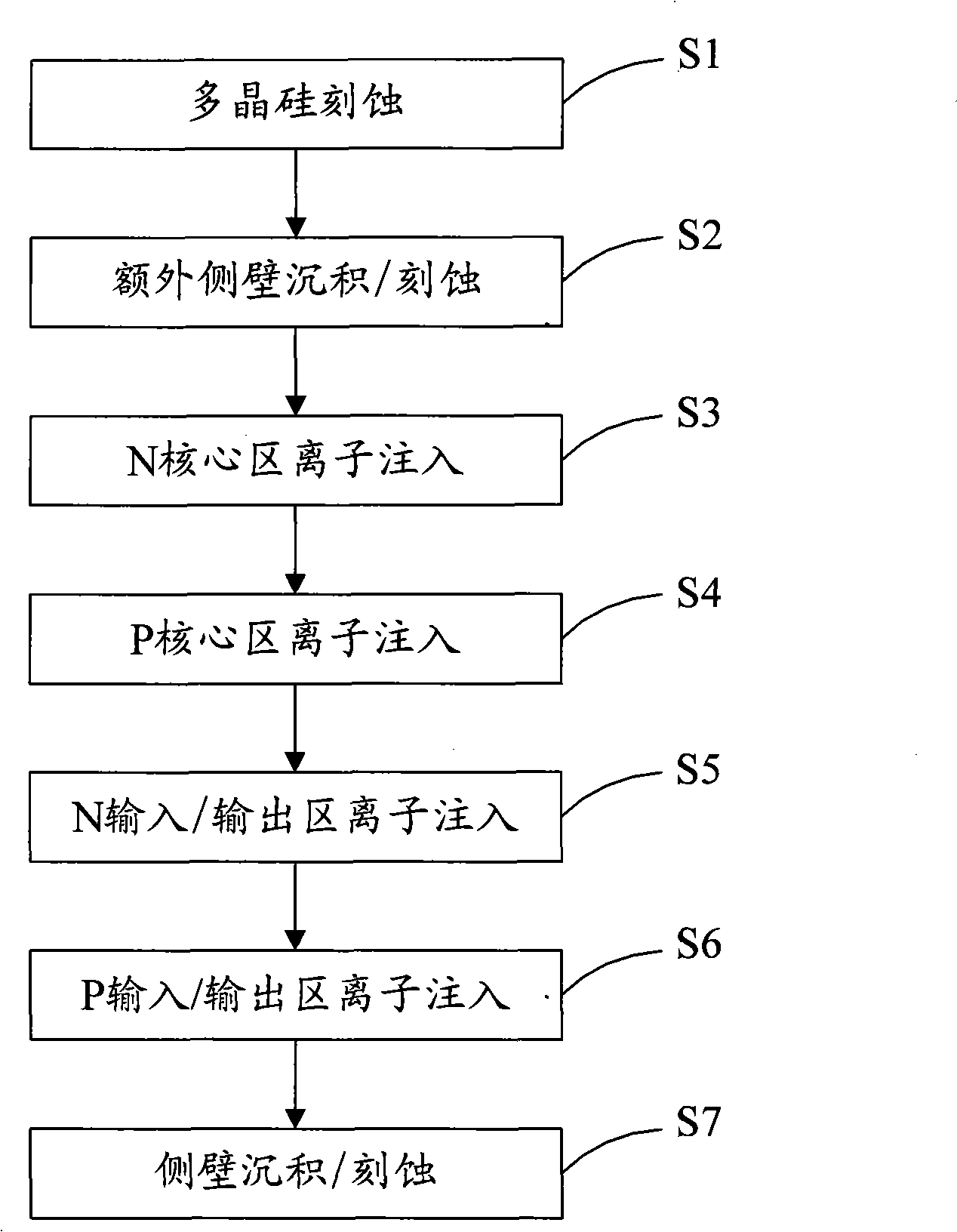
[0012] The manufacturing method of the input / output device of the present invention will be further described in detail below.

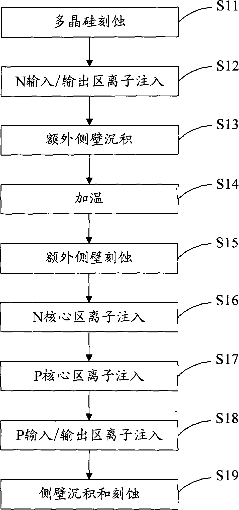
[0013] The biggest difference between the method of the present invention and the prior art is that the N I / O ion implantation step is performed in advance before additional sidewall deposition / etching. There are two reasons for advancing this step: 1) The hot carrier effect has a greater impact on N, but relatively less impact on P; 2) The working voltage of the I / O area is higher than that of the Core area, and it is more susceptible to heat load flow effect. Therefore, N I / O ion implantation is advanced.

[0014] see figure 2 In the method of the present invention, after polysilicon etching S11 is completed, step S12, N I / O ion implantation, is performed first, and the ion implantation used in the present invention is lightly doped drain (Light Doped Drain, LDD) ion implantation, and then, An additional sidewall deposition step S13 is performe...


PUM


Abstract

The invention discloses a manufacturing method of an input / output device, which relates to a manufacturing process of a semi-conducting device. An I / O device manufactured by the using existing process is easily affected by hot carrier effect in a condition of high voltage. The manufacturing method of the invention comprises the following steps of: a. ion implantation of N input / output area; b. extra side wall deposition; c. heating; d. extra side wall etching; e. ion implantation of N core area; f. ion implantation of P core area; g. ion implantation of P input / output area; h. side wall deposition and etching. By putting the step of N I / O ion implantation ahead of the step of extra side wall deposition and adding the step of heating between the step of extra side wall deposition and the step of extra side wall etching, the manufacturing method can effectively utilize instantly increased diffusion effect to form graded junction, thus improving the hot carrier effect. By adopting the I / O device manufactured by the method of the invention, the influences of the hot carrier effect on the device can be effectively avoided.

Description

technical field [0001] The invention relates to a manufacturing process of a semiconductor device, in particular to a method for improving the hot carrier reliability of an input / output device. Background technique [0002] When a high-voltage input / output (I / O) device operates in a saturated current state, the charges in the inversion layer are accelerated under the action of the lateral electric field on the channel surface and collide with the crystal lattice to generate a large number of hot carriers. The generated hot carriers will be injected into the gate dielectric layer under the action of the surface gate-drain electric field, forming a hot-carrier injection (HCI), which will seriously affect the operating characteristics and reliability of the device. When the operating voltage of the input / output device is higher, it is more obviously affected by the hot carrier effect. With the continuous development of technology, the feature size of devices is decreasing day ...

Claims


Application Information

Patent Timeline
Patent Type & Authority Applications(China)
IPC IPC(8): H01L21/04H01L21/18H01L21/336
Inventor 丁宇居建华
Owner SEMICON MFG INT (SHANGHAI) CORP
Features
  • R&D
  • Intellectual Property
  • Life Sciences
  • Materials
  • Tech Scout
  • Unparalleled Data Quality
  • Higher Quality Content
  • 60% Fewer Hallucinations
Learn More