Liquid crystal display device and method of fabricating the same

A liquid crystal display and device technology, applied in the field of liquid crystal display devices and their manufacturing, can solve the problems of processing time and cost burden

Active Publication Date: 2009-01-14
LG DISPLAY CO LTD
View PDF0 Cites 25 Cited by
  • Summary
  • Abstract
  • Description
  • Claims
  • Application Information

AI Technical Summary

Problems solved by technology

Because the use of liquid crystals, especially in the manufacture of panels, creates a large burden in terms of processing time and cost, efforts are required to reduce the amount of liquid crystals used

Method used


Image

  • Liquid crystal display device and method of fabricating the same
  • Liquid crystal display device and method of fabricating the same
  • Liquid crystal display device and method of fabricating the same

Examples


Embodiment Construction

[0081] Reference will now be made in detail to the preferred embodiments of the invention, examples of which are illustrated in the accompanying drawings. Wherever possible, the same reference numbers will be used throughout the drawings to refer to the same or like parts.

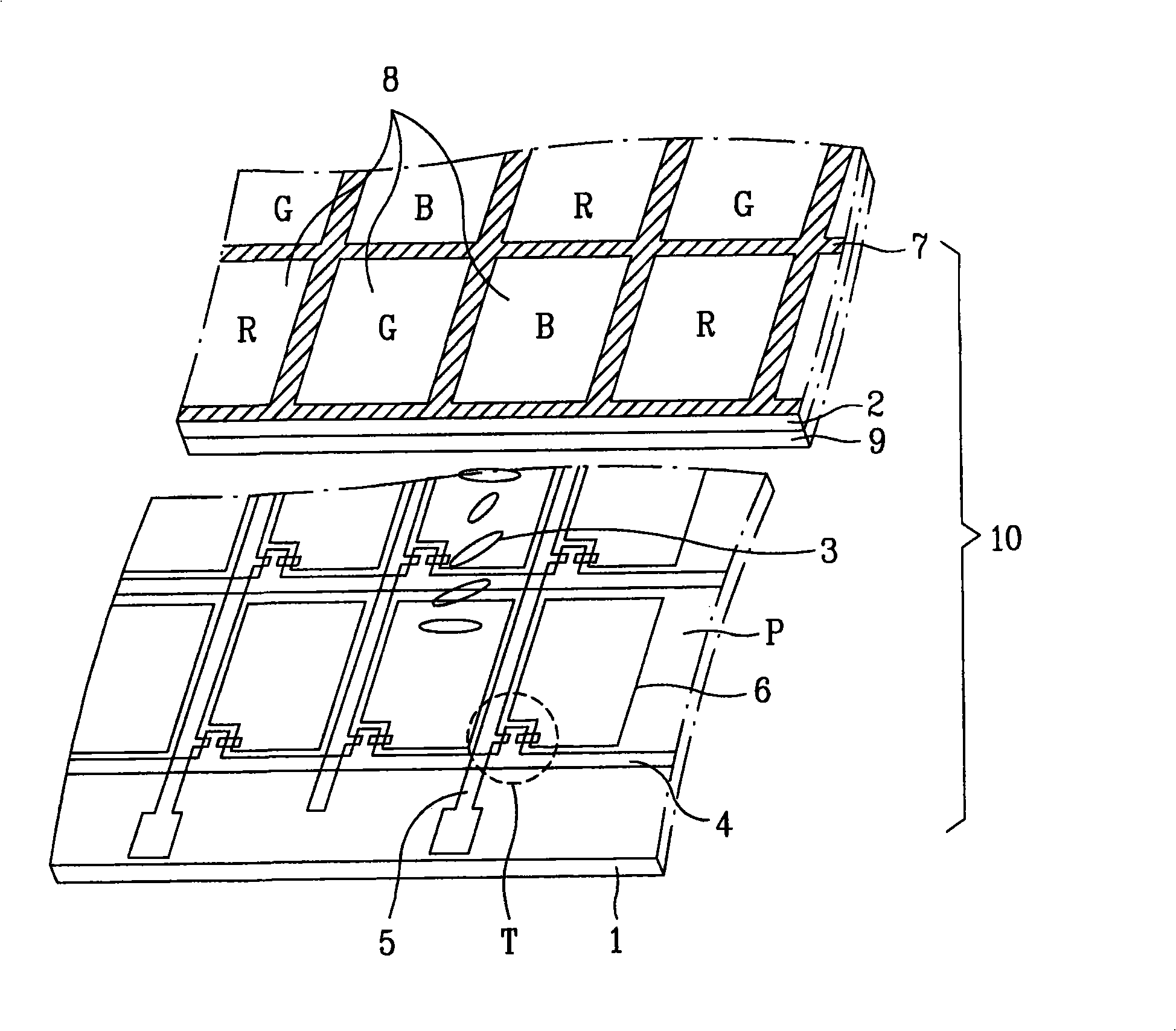
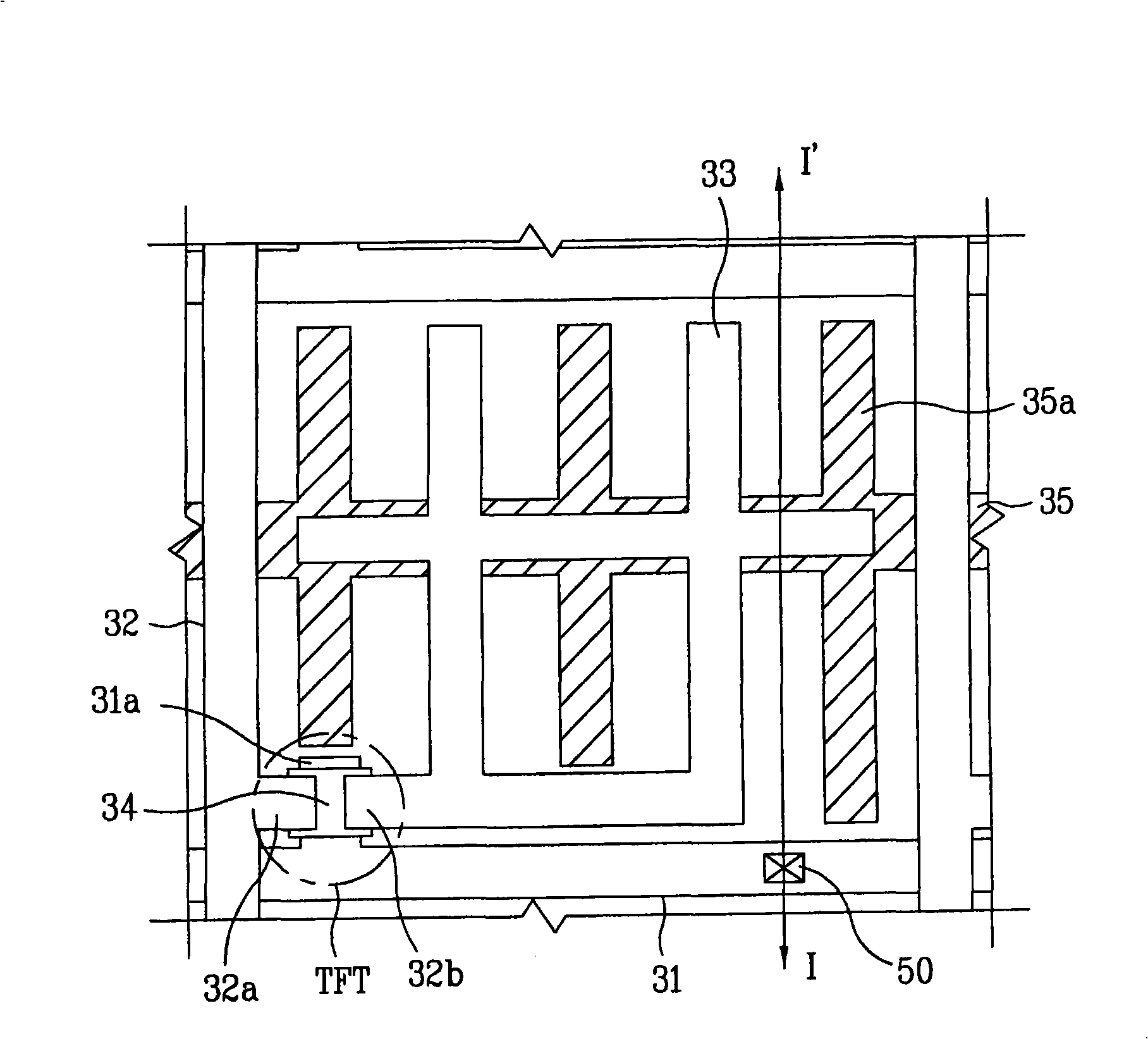
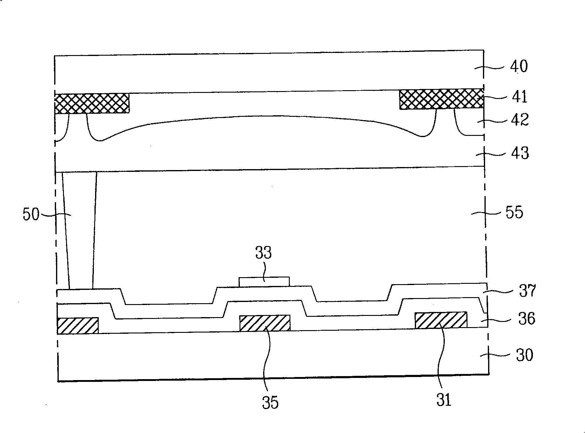
[0082] Figure 4 Shown is a plan view of one pixel of a liquid crystal display (LCD) device according to the present invention, wherein a columnar spacer and a spacer pattern are formed corresponding to the pixel, and Figure 5 shown along Figure 4 The cross-sectional views extracted by lines II-II′, III-III′ and IV-IV′.

[0083] like Figure 4 and Figure 5 As shown, each pixel of the LCD device according to the present invention includes R, G and B sub-pixels. Each sub-pixel includes gate lines ( Image 6 "151") and data line ( Image 6 "155a" in ). The gridlines are shown extending in the horizontal direction. In each sub-pixel, where the sub-pixel is divided in half into a region having a verti...


PUM

PropertyMeasurementUnit
widthaaaaaaaaaa
widthaaaaaaaaaa

Abstract

The present invention discloses a liquid crystal display device and the manufacturing method thereof, which can reduce the used liquid crystal quantity in the liquid crystal device according to the special column wadding forming technique. A liquid crystal display device includes first and second substrates facing each other; gate lines and data lines formed on the first substrate such that the gate lines and the data lines intersect each other to define pixel regions; thin film transistors formed at respective intersections of the gate lines and the data lines; a black matrix layer formed on the second substrate such that the black matrix layer corresponds to a region other than the pixel regions; color filter layers extending in an extension direction of the data lines in respective pixel regions; a liquid crystal layer interposed between the first and second substrates; first column spacers formed on one of the first and second substrates such that each first column spacer corresponds to an associated one of the gate lines or to a channel region of an associated one of the thin film transistors to maintain a cell gap between the first-and second substrate; and spacer patterns formed on one of the first and second substrates such that each spacer pattern corresponds to at least one of an associated one of the gate lines and an associated one of the data lines, thereby forming a first gap between the spacer pattern and the other substrate facing the spacer pattern, and reducing an amount of liquid crystals filled between the first and second substrates.

Description

[0001] This application claims priority from Patent Application No. 10-2007-070253 filed in Korea on July 12, 2007 and Patent Application No. 10-2007-098684 filed in Korea on October 1, 2007, the entire contents of which are incorporated Here for reference. technical field [0002] The present invention relates to a liquid crystal display device, and more particularly, to a liquid crystal display device and a method of manufacturing the same, which can reduce the amount of liquid crystal used in the liquid crystal display device according to a specific column spacer forming process. Background technique [0003] With the development of an information-dependent society, the demand for various display devices is increasing. In order to meet such demands, a great deal of effort has recently been devoted to developing flat panel display devices such as liquid crystal display (LCD) devices, plasma display panels (PDP), electroluminescent display (ELD) devices, vacuum fluorescent ...

Claims


Application Information

Patent Timeline
Patent Type & Authority Applications(China)
IPC IPC(8): G02F1/1339G02F1/1362G02F1/133
CPCG02F1/133512G02F1/1339G02F1/136286H01L29/786
Inventor 崔荣锡郑裕澔李尚镕
Owner LG DISPLAY CO LTD
Why Eureka
Try Eureka