Method for manufacturing parasitic NPN transistor and structure thereof

A manufacturing method and transistor technology, which is applied in the direction of transistor, semiconductor/solid-state device manufacturing, electrical components, etc., can solve the problems of parasitic transistor application limitations, affecting the performance of other devices, etc., and achieve the effect of improving the amplification gain

Active Publication Date: 2009-01-21
SHANGHAI HUAHONG GRACE SEMICON MFG CORP
View PDF0 Cites 7 Cited by
  • Summary
  • Abstract
  • Description
  • Claims
  • Application Information

AI Technical Summary

Problems solved by technology

However, if you want to adjust the amplification gain of the parasitic transistor, it will affect the performance of other devices, so the ability of the parasitic transistor is generally sacrificed to ensure that the performance of the entire device is not affected, which limits the application of the parasitic transistor

Method used


Image

  • Method for manufacturing parasitic NPN transistor and structure thereof
  • Method for manufacturing parasitic NPN transistor and structure thereof

Examples


Embodiment Construction

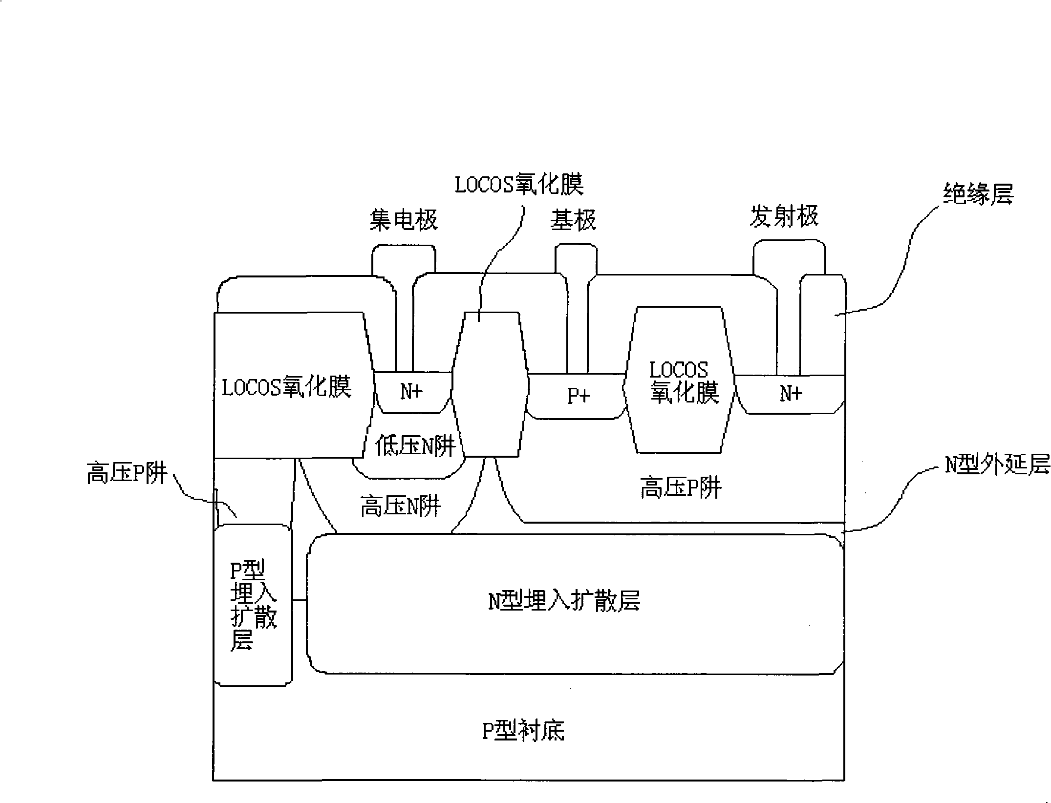
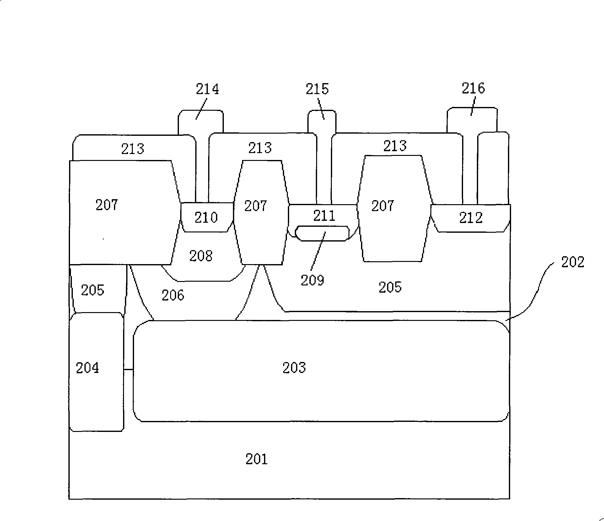
[0018] control figure 2 , in one embodiment, in order to improve the amplification gain of the parasitic NPN transistor, it can be manufactured by the following method:

[0019] In the first step, a P-type single crystal silicon substrate 201 is prepared. Then, using a known photolithography technique, N-type impurities such as As (arsenic) or Sb (antimony) are implanted and diffused from the surface of the substrate 201 to form an N-type buried diffusion layer 203 . Next, P-type impurities, such as boron (B) plasma, are implanted and diffused from the surface of the substrate 201 using known photolithography techniques to form a P-type buried diffusion layer 204 .

[0020] In the second step, since the N-type buried diffusion layer 203 is advanced, a layer with a thickness of about 2300~ Therefore, in this step, it is necessary to use a wet method (such as chemical reagent hydrofluoric acid, etc.) to remove the buried oxide layer, and then place the substrate 201 on the s...


PUM


Abstract

The invention discloses a process for preparing a parasitic NPN transistor and a structure thereof, wherein the structure of the NPN transistor is changed through implanting N type foreign mater through adopting the light doping technique ion implantation in a base region window of a NPN transistor, which is equal to that a longitudinal PNP transistor is generated in the structure, thereby the improvement of the amplification gain of the parasitic NPN transistor can be realized without affecting the performances of other devices in a BCD / BICOM device. In the method, the step for implanting the N type foreign matter by the ion implantation comprises two processes for implanting ion, namely a process for implanting P type foreign matter through adopting the ion implantation with the light doping technique, and a process for implanting N type foreign matter through adopting the ion implantation with the large-angle technique.

Description

technical field [0001] The present invention relates to a manufacturing method of a parasitic NPN transistor; therefore, the present invention also relates to a parasitic NPN transistor formed by using the manufacturing method. Background technique [0002] For BICMOS / BCD devices, due to the limitation of the process flow, most bipolar transistors use the parasitic method to realize their structure, and its structure is as follows figure 1 shown. However, if the amplification gain of the parasitic transistor is to be adjusted, the performance of other devices will be affected. Therefore, the capability of the parasitic transistor is generally sacrificed to ensure that the performance of the entire device is not affected, which limits the application of the parasitic transistor. Contents of the invention [0003] The technical problem to be solved by the present invention is to provide a method for manufacturing a parasitic NPN transistor, which can effectively improve the...

Claims


Application Information

Patent Timeline
Patent Type & Authority Applications(China)
IPC IPC(8): H01L21/331H01L21/265H01L29/73
Inventor 王乐雷明
Owner SHANGHAI HUAHONG GRACE SEMICON MFG CORP
Why Eureka
Try Eureka