

Method for manufacturing micromechanical components
A micro-mechanical component and micro-mechanical technology, applied in the manufacture of micro-structure devices, electrical components, micro-structure technology, etc., can solve problems such as limiting the thickness of structural layers
- Summary
- Abstract
- Description
- Claims
- Application Information
AI Technical Summary
Problems solved by technology
Method used
Image

Examples
Embodiment Construction
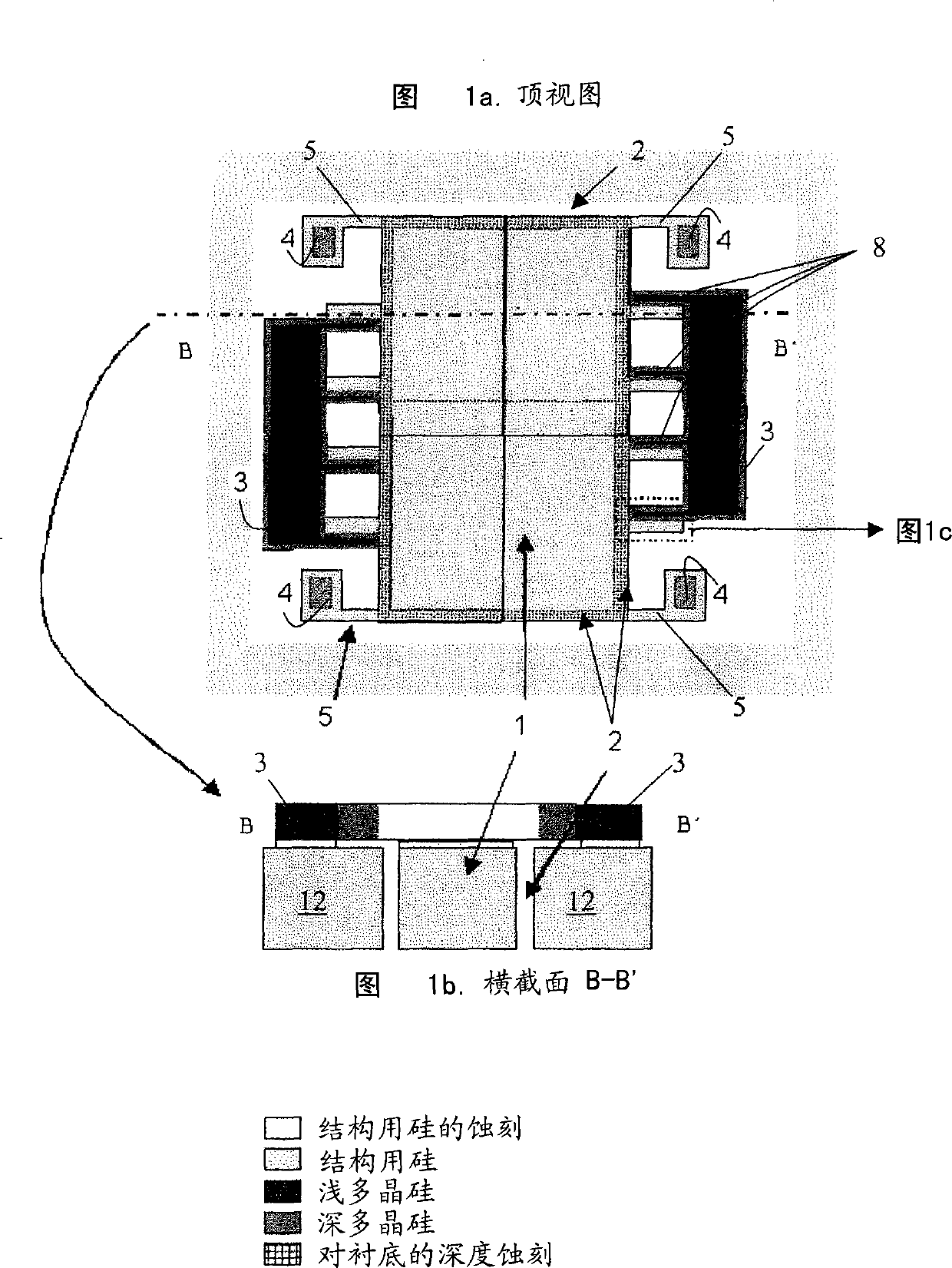
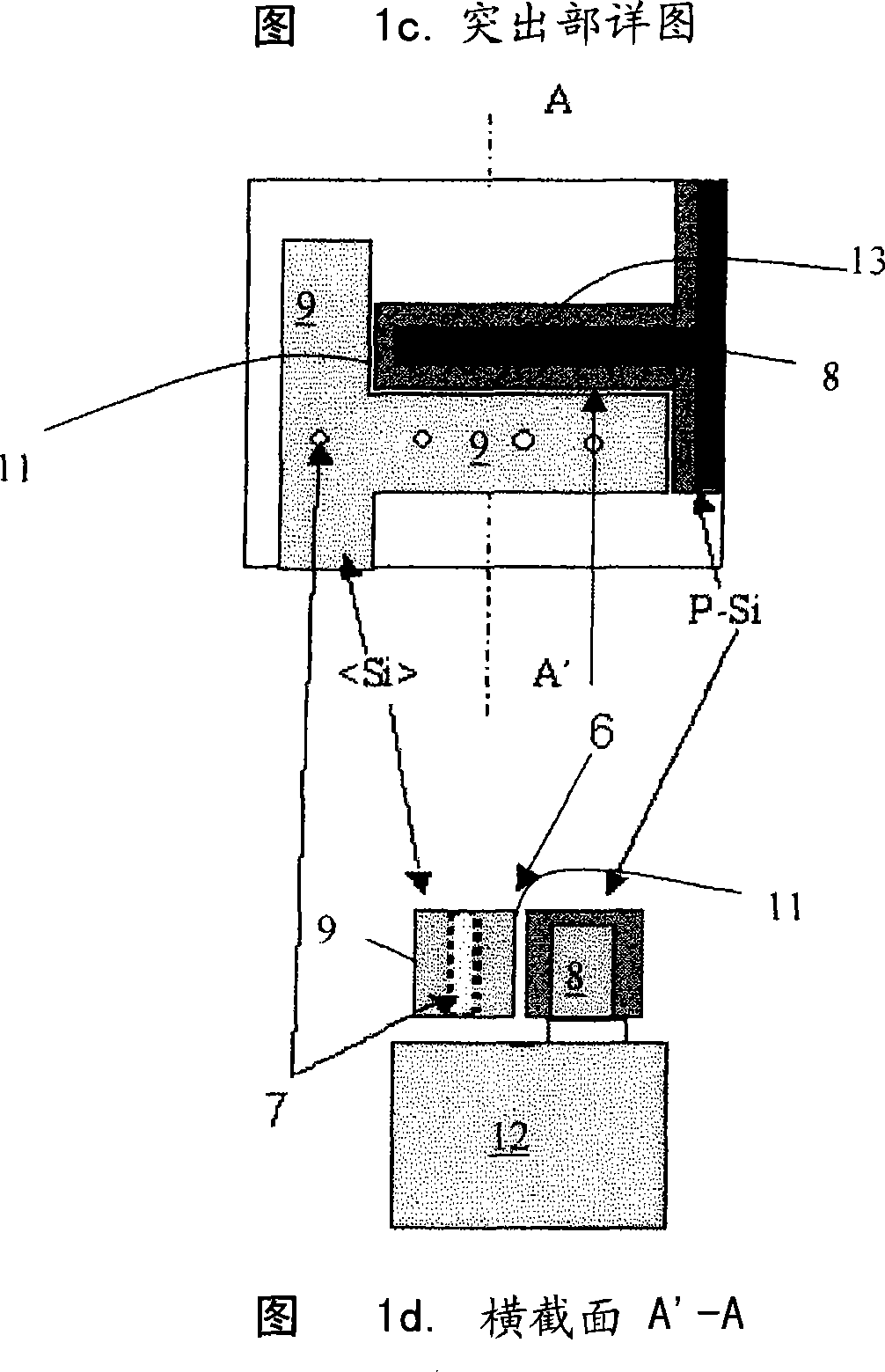
[0050] In FIG. 1 , a movable structure 1 made of monocrystalline silicon “floats” on four anchors 4 to which it is attached by means of suspension springs 5 . A groove 2 is provided around the movable structure 1 , which groove ensures the mobility of said structure by separating the movable structure 1 from the substrate 12 . Detection holes 7 are also provided in single crystal silicon for release etching. In monocrystalline silicon, there are at least two protrusions 9, while a corresponding number of electrode protrusions 8 are arranged relative to them. Between the protrusion 9 and the electrode protrusion 8 of the monocrystalline silicon, a narrow gap 6 is etched, which is formed by a longitudinal groove 11 and a transverse groove 13 , and forms a gap in which the junction capacitance is formed by the protrusions 8 , 9 . The protrusions give the electrode structure a comb-like profile when viewed from above.
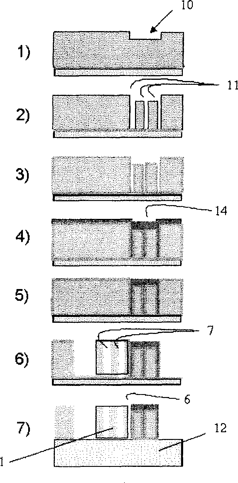
[0051] figure 2The individual steps (steps 1-7) of a ma...
PUM
| Property | Measurement | Unit |
|---|---|---|
| width | aaaaa | aaaaa |
| width | aaaaa | aaaaa |
| thickness | aaaaa | aaaaa |
Abstract
Description
Claims
Application Information