Method for manufacturing chip inductor and inductor thereof

A manufacturing method and inductor technology, applied in the manufacture of inductors/transformers/magnets, inductors, fixed inductors, etc., can solve the problems of large material consumption, low pass rate, and high cost

Inactive Publication Date: 2009-01-28
GUANGDONG FENGHUA ADVANCED TECH HLDG
View PDF1 Cites 17 Cited by
  • Summary
  • Abstract
  • Description
  • Claims
  • Application Information

AI Technical Summary

Problems solved by technology

However, this method consumes a lot of materials, costs are high, and equipment investment is large.
[0004] All-wet production method: make ferrite or ceramic dielectric materials plus adhesives to make a slurry suitable for cascade flow, flow a certain thickness of diaphragm on the carrier plate under mechanical drive, and then print the conductive wire electrode slurry, Then print the inter-turn connection paste on the wire electrode and form a bump. When the flow medium diaphragm is used, the diaphragm will form a connection through hole at the bump, and then print a conductive wire electrode on the through hole to make the inter-turn connection good. Repeatedly form an inductor structure with a certain thickness, and then dry, cut, deglue, sinter, seal, electroplate, test and inspect, but this method has high material costs, and the production efficiency drops significantly when making small-scale products, and the pass rate is low. , Poor performance reliability

Method used


Image

  • Method for manufacturing chip inductor and inductor thereof
  • Method for manufacturing chip inductor and inductor thereof

Examples


Embodiment

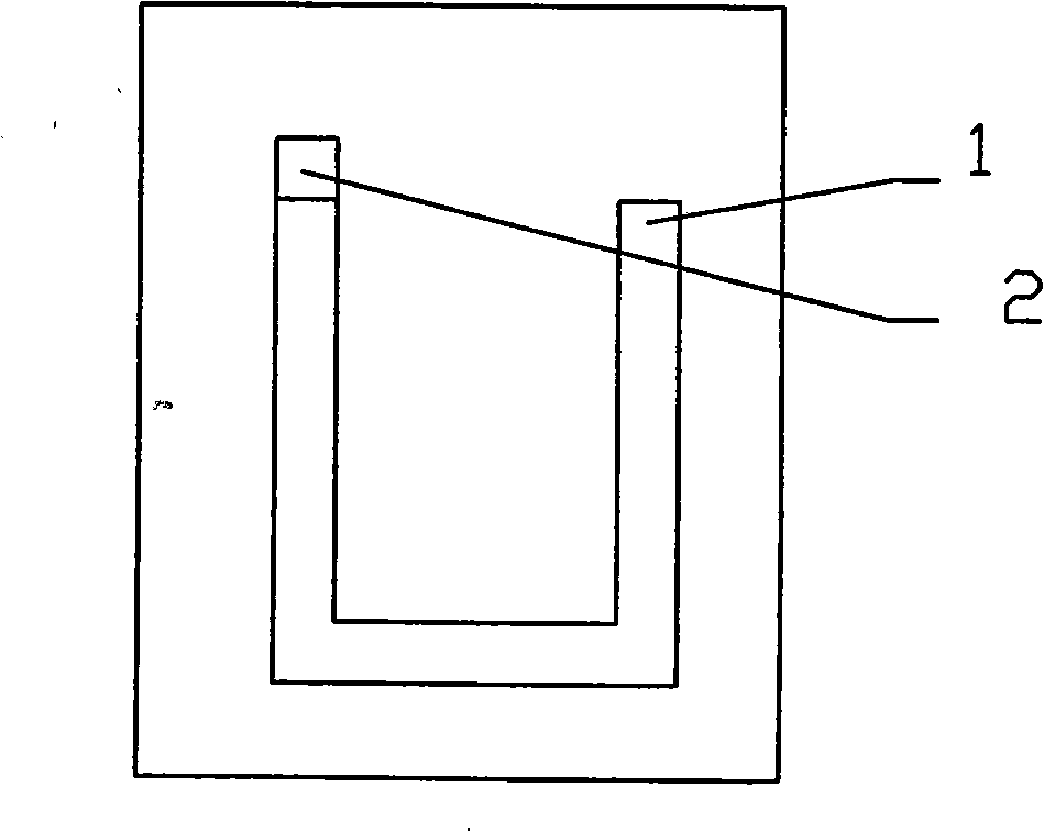
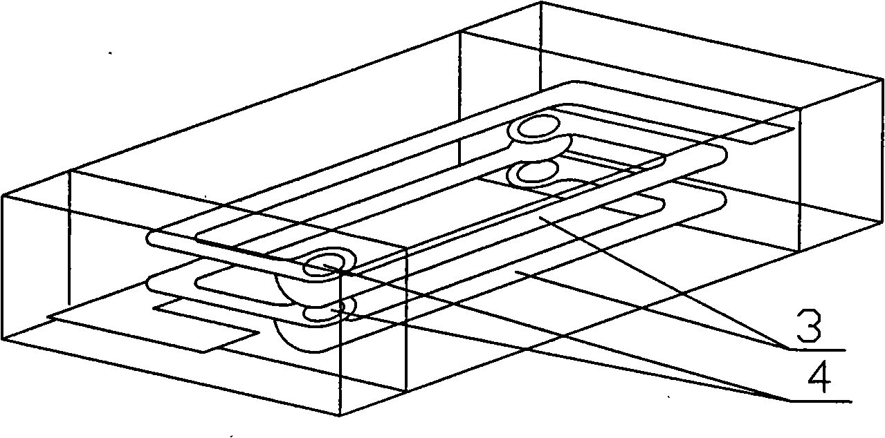
[0018] A method for manufacturing a chip inductor, comprising the steps of screen printing, tape casting, glue removal, and sintering. In the screen printing step, the wire groove of the screen printing frame is 0.5 to 0.85 weeks, preferably 0.75 weeks. There is a photosensitive latex column 2 at one end of the wire groove 1; a screen printing frame is placed on the base casting die, and a wire conductor paste is printed on the wire groove of the frame to form an internal electrode 3; The dielectric paste is printed on the frame surface to form a dielectric die. Since the photosensitive emulsion column blocks the dielectric slurry, a through hole is formed at the photosensitive emulsion column; that is, during the printing transfer process, there is no dielectric paste at the connection of the internal electrode, forming A through hole not covered with dielectric paste, so that when the next layer of electrode paste is printed, the paste automatically flows into the through ho...


PUM

PropertyMeasurementUnit
particle sizeaaaaaaaaaa
specific surface areaaaaaaaaaaa

Abstract

The invention discloses a method for manufacturing a chip inductor, which comprises the steps of screen printing, casting, glue removal and sintering; in the step of screen printing, a conducting wire groove of a screen printing frame is between 0.5 and 0.85 circle; one end of the conducting wire groove is provided with a light sensing latex column; the screen printing frame is positioned on a substrate casting membrane; a line conductor sizing agent is printed on the conducting wire groove of the frame to form an inner electrode; a medium sizing agent is printed on the whole screen printing frame surface to form a medium membrane; pylomes are formed in the light sensing latex column; the screen printing frame is repeatedly positioned; the line conducting wire sizing agent and the medium sizing agent are printed to form a magnetic body of the chip inductor. The method reduces production cost and equipment input and improves production efficiency and the qualification rate of producing the inductor with ultra-small size. The inductor manufactured by the method has reliable performance.

Description

technical field [0001] The invention relates to a method for manufacturing an inductor and the obtained inductor, in particular to a method for manufacturing an ultra-small laminated inductor and the obtained inductor. Background technique [0002] At present, the production methods of multilayer chip inductors at home and abroad generally have the following types, and the principles and characteristics are different. Alternate printing wet method: make ferrite or ceramic dielectric materials plus adhesives and other pastes suitable for screen printing and print them into dielectric films. After the printed dielectric film reaches a certain thickness, print 0.5 to 0.75 Conductive electrodes around the circle, and then print a dielectric film on half of the entire area, so that 1 / 2 of the upper layer of electrodes is covered by the dielectric film, and then continue to print 0.5 to 0.75 weeks of conductive electrodes, connected to the previous electrode, and repeatedly form i...

Claims


Application Information

Patent Timeline
Patent Type & Authority Applications(China)
IPC IPC(8): H01F17/00H01F41/00
Inventor 陈加旺李强徐建平车琦文
Owner GUANGDONG FENGHUA ADVANCED TECH HLDG
Why Eureka
Try Eureka