Exposure apparatus, exposure method, and method for manufacturing display panel substrate

A technology of exposure device and exposure method, which is applied in the direction of exposure device for photo-plate-making process, photo-plate-making process for pattern surface, micro-lithography exposure equipment, etc., to achieve the effect of high-precision positioning

CN101359185AInactive Publication Date: 2009-02-04HITACHI HIGH-TECH CORP
2 Cites 3 Cited by

Patent Information

Authority / Receiving Office
CN · China
Patent Type
Applications(China)
Current Assignee / Owner
Publication Date
2009-02-04
Estimated Expiration
Not applicable · inactive patent

Smart Images

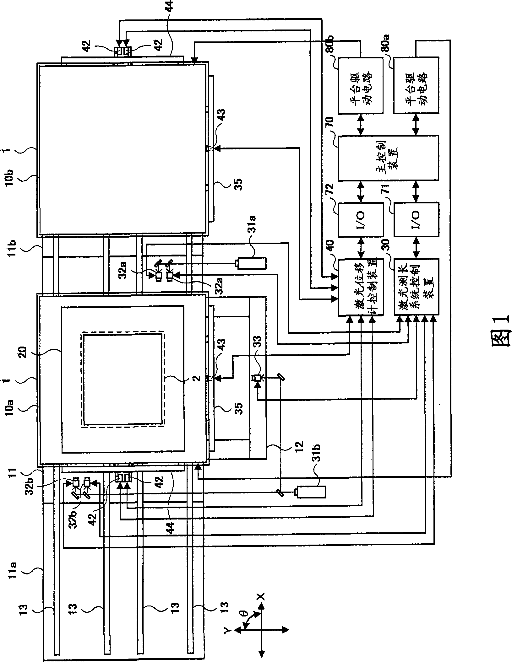
  • Figure 1
    Figure 1
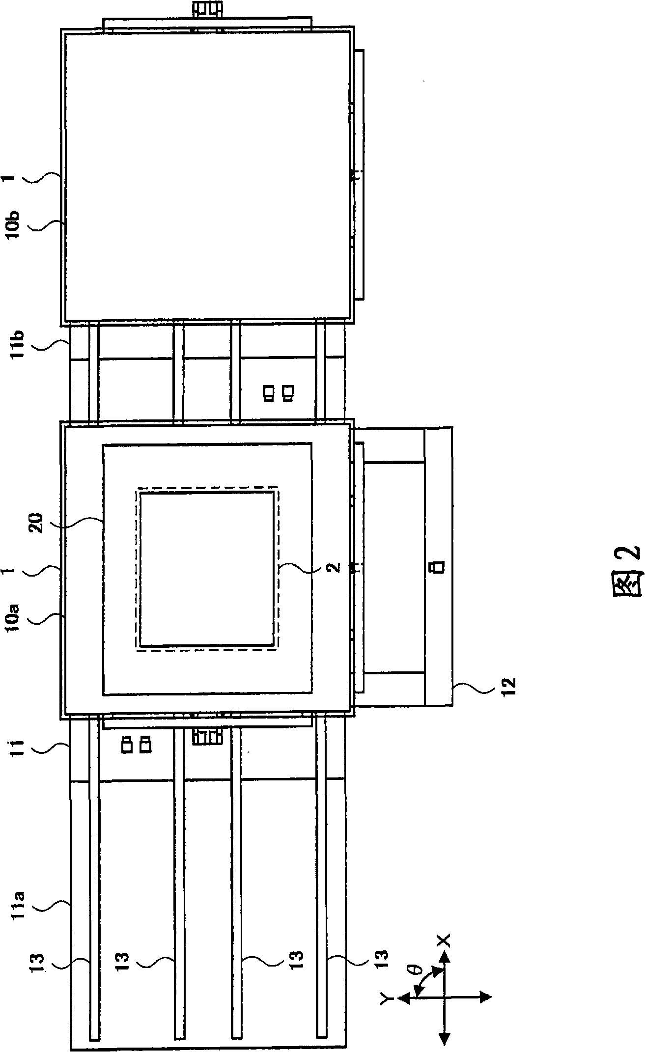
  • Figure 2
    Figure 2
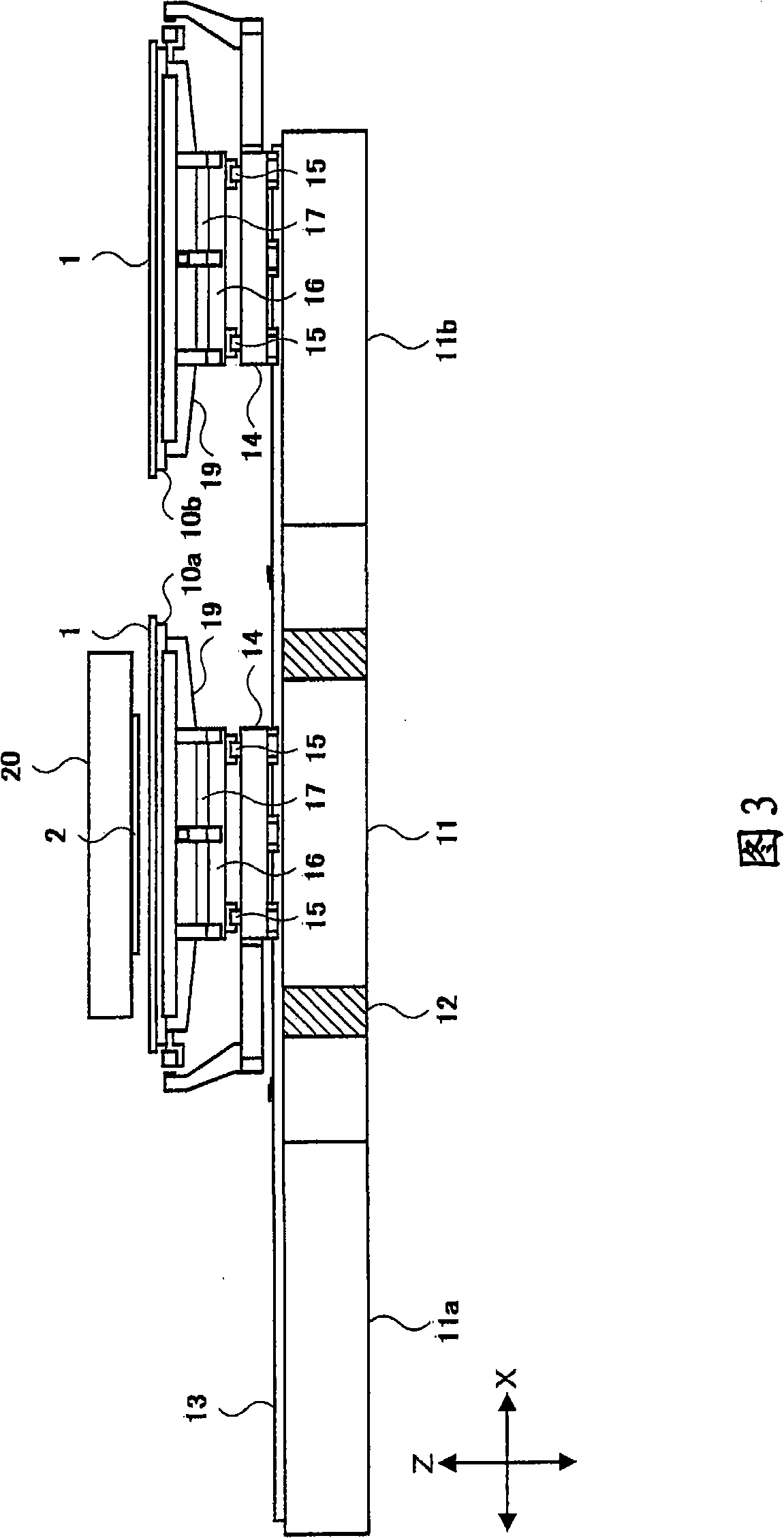
  • Figure 3
    Figure 3
Patent Text Reader

Abstract

In exposure in an approximate method by using a plurality of mobile states, a laser distance-to-coupling measurement device is used, to perform position of the sustrate in exposure with high precision. The movable stages carry chucks 10a and 10b and move towards secondary stage bases 11a and 11b and a primary stage base 11, thereby positioning the substrate 1 on the primary stage base 11. Each first laser length-measuring system includes laser sources 31a and 31b, bar mirrors 34a and 34b mounted below X stages 14 of the movable stages, and laser interferometers 32a and 32b disposed at positions deviated from X guide rails 13 on the primary stage base 11, so as to detect positions of the movable stages in X direction. The laser interferometers 32a and 32b will not be influenced by the vibration of the secondary stage bases 11a and 11b. Meanwhile, the measuring distance from the laser interferometers 32a and 32b to the movable stages on the primary stage base 11 is reduced.
Need to check novelty before this filing date? Find Prior Art

Description

technical field

[0001] The present invention relates to an exposure device and an exposure method for exposing a substrate using a proximity method when manufacturing a display panel substrate such as a liquid crystal display device, and a display panel substrate using the exposure device and the exposure method. The manufacturing method particularly relates to an exposure apparatus including a plurality of moving stages, an exposure method, and a method for manufacturing a display panel substrate using the exposure apparatus and the exposure method. Background technique

[0002] Thin Film Transistor (TFT) substrates, color filter (color filter) substrates, plasma display panel (plasma display panel) substrates, organic electroluminescence (Electroluminescence) , EL) display panel substrates, etc., are produced by forming a pattern on a substrate by a photolithography technique using an exposure device. The exposure device has a projection method and a proximity method. The...

Examples

Embodiment Construction

[0062] In order to further explain the technical means and effects of the present invention to achieve the intended purpose of the invention, the exposure device, the exposure method and the manufacturing method of the panel substrate for display according to the present invention are described in detail below in conjunction with the accompanying drawings and preferred embodiments. Embodiments, structures, methods, steps, features and effects thereof are described in detail below.

[0063] FIG. 1 is a diagram showing a schematic configuration of an exposure apparatus according to an embodiment of the present invention. The exposure device includes a plurality of chucks 10a and 10b, a main platform base 11, a plurality of sub-platform bases 11a and 11b, a pedestal 12, an X guide rail 13, a plurality of moving platforms, a mask frame 20, a laser length measuring system control device 30, Multiple first laser length measuring systems, second laser length measuring systems, laser ...