Method for marking wafer, method for marking poor product crystal grain, method for wafer contraposition, and wafer test machine

A wafer testing and wafer technology, which is used in semiconductor/solid-state device testing/measurement, laser welding equipment, electrical components, etc., and can solve problems such as difficulty in identification, difficult control of ink dot size, and easy contamination of wafers.

Inactive Publication Date: 2009-02-18
KING YUAN ELECTRONICS
View PDF0 Cites 40 Cited by
  • Summary
  • Abstract
  • Description
  • Claims
  • Application Information

AI Technical Summary

Problems solved by technology

[0007] In view of the above problems, an object of the present invention is to solve problems such as the difficulty in controlling the size of ink dots in the existing ink marking process, the easy contamination of wafers, and the long operating time. However, due to the shortening of operating time, the number of machines required It is also reduced, which can effectively save the workshop space
[0009] Another object of the present invention is to propose a method for permanently marking wafers or inferior grains to effectively solve the problem that existing ink marks are easily blurred or difficult to identify due to factors such as the environment or time, so that the wafer must be washed The problem of re-marking the process afterward

Method used


Image

  • Method for marking wafer, method for marking poor product crystal grain, method for wafer contraposition, and wafer test machine
  • Method for marking wafer, method for marking poor product crystal grain, method for wafer contraposition, and wafer test machine
  • Method for marking wafer, method for marking poor product crystal grain, method for wafer contraposition, and wafer test machine

Examples


Embodiment Construction

[0057] The present invention enumerates some embodiments in detail as follows, wherein the related icons are not drawn according to the actual style or proportion, and their function is only to facilitate the expression of the characteristics of the present invention, and for the sake of concise content, the same marked symbols in the description indicate that they have Components with the same function. In addition, the examples provided below are only for convenience of explaining the technical characteristics of the present invention, and the scope of the present invention is not limited by the provided examples, but is subject to the claims of the present invention.

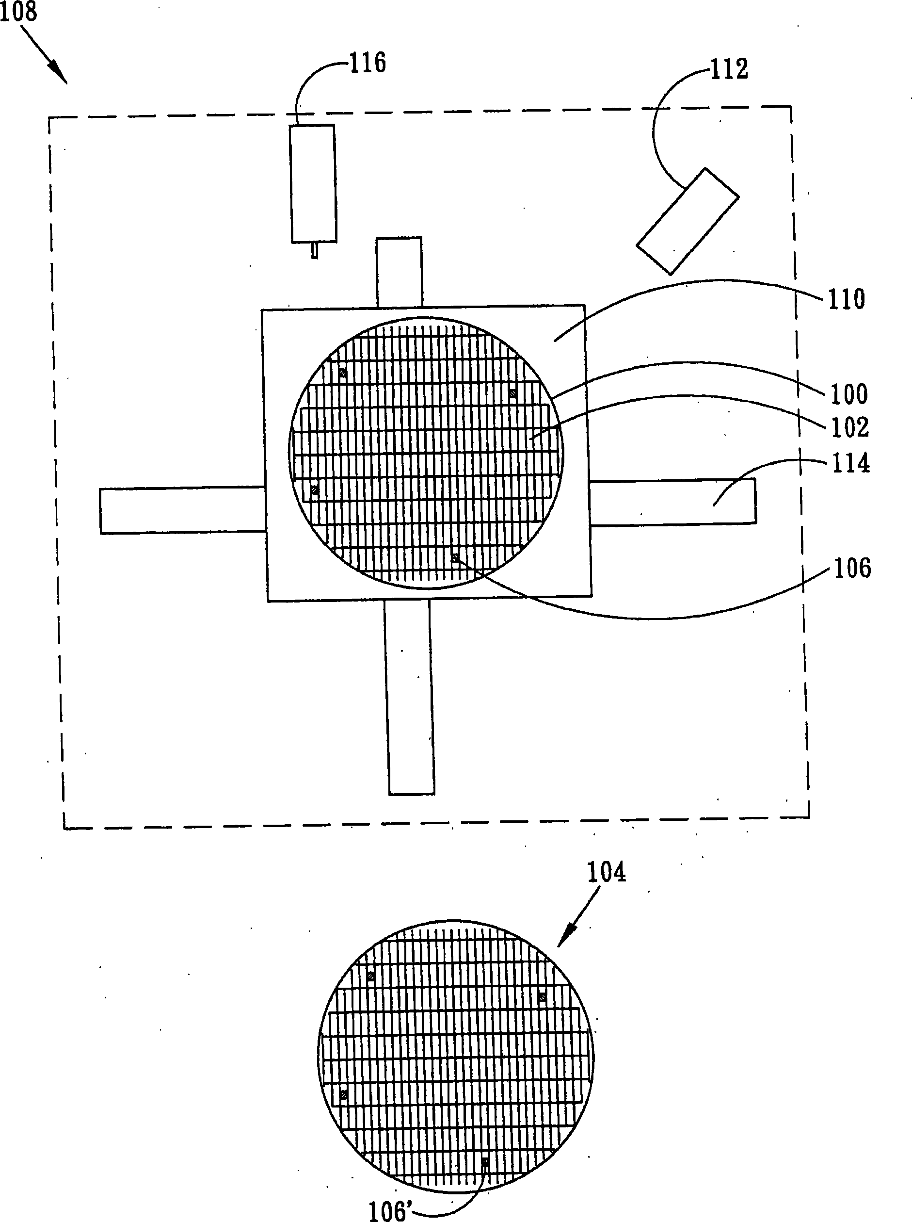
[0058] First, an embodiment of the present invention provides a wafer marking process, which uses lasers for wafer marking, and is combined with the wafer alignment method provided by the present invention to save the time for wafer alignment and improve wafer alignment. The accuracy of the circle alignment i...


PUM

PropertyMeasurementUnit
wavelengthaaaaaaaaaa

Abstract

The invention provides a method for marking a wafer, which comprises providing a wafer having at least two reference marks, wherein a surface of the wafer comprises a plurality of crystal grains, at the same time, detecting the reference marks of the wafer to perform a wafer alignment, and marking the wafer by a laser. In addition, the invention can be suitable for marking the crystal grains of the wafer (for example, throwout crystal grains), comparing to the prior art of marking the throwout crystal grains by ink, has advantages of less wafer pollution, operation time, workshop space and permanent marker, is easier to reconstruct by the existing wafer tester or ink machine platform.

Description

technical field [0001] The invention relates to a method for marking a wafer, and in particular relates to a method for marking inferior crystal grains by using laser light. Background technique [0002] The general integrated circuit manufacturing process can be divided into the wafer manufacturing stage, the die testing stage and the die packaging stage in sequence. As the current electronic products are light and thin, the current packaging technology is designed to reduce the packaging volume and improve the performance of integrated circuits. It has gradually tended to high-end packaging technologies such as flip-chip packaging and multi-chip modules. However, these high-end packaging methods are expensive. These inferior chips are eliminated to save unnecessary packaging costs. [0003] A wafer-free ink dot test method can generate a wafer image (MAP) after the wafer test, as the basis for the packaging of each die. The method of die marking is easy to cause mistakes...

Claims


Application Information

Patent Timeline
Patent Type & Authority Applications(China)
IPC IPC(8): H01L21/00H01L21/68H01L21/66B41M5/24B23K26/00B23K26/06
Inventor 郑匡文
Owner KING YUAN ELECTRONICS
Why Eureka
Try Eureka