Production method and apparatus for single-slice integrated semiconductor laser array

A laser array, monolithic integration technology, applied in the field of optoelectronics, can solve problems such as the influence of lasing characteristics and the failure of lasers to work normally, and achieve the effects of reducing production costs, reducing manufacturing difficulty, and improving device performance

Active Publication Date: 2009-02-18
NANJING UNIV
View PDF7 Cites 45 Cited by
  • Summary
  • Abstract
  • Description
  • Claims
  • Application Information

AI Technical Summary

Problems solved by technology

Because, even if the built-in phase shift can ensure that the laser works in a single mode near the threshold current, as the injection current increases, the side mode suppression ratio of the laser decreases, and the longitudinal mode space hole burning effect occurs, resulting in the phenomenon of multiple longitudinal modes in the laser. unable to work p

Method used


Image

  • Production method and apparatus for single-slice integrated semiconductor laser array
  • Production method and apparatus for single-slice integrated semiconductor laser array
  • Production method and apparatus for single-slice integrated semiconductor laser array

Examples


Embodiment Construction

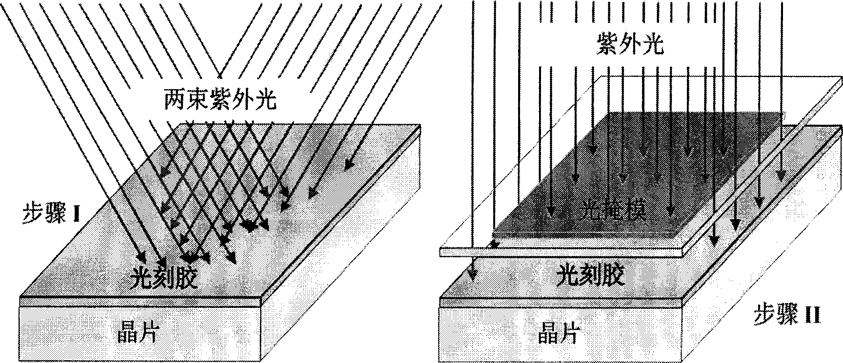
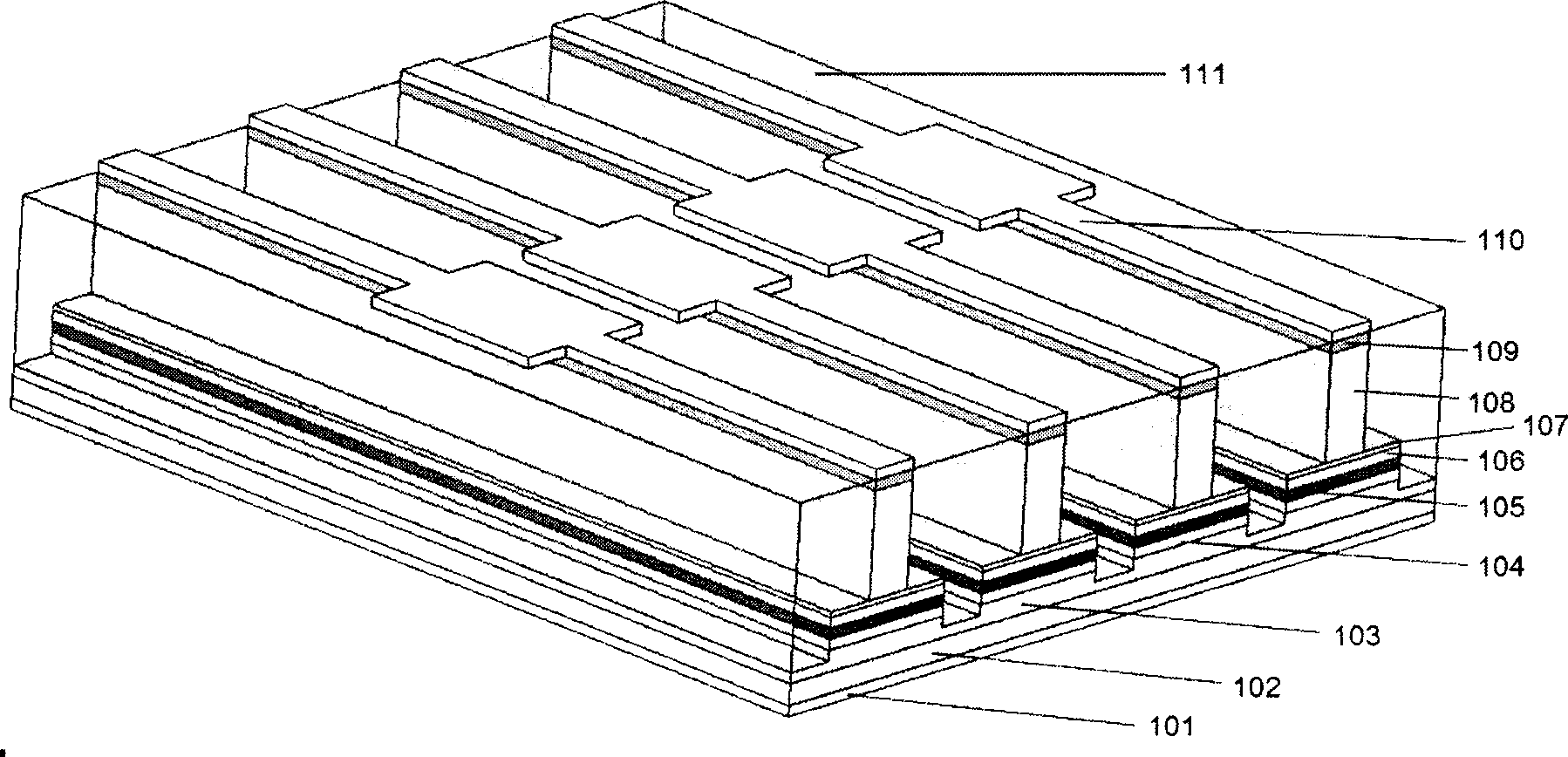
[0039] The structure of the distributed feedback semiconductor laser is that on the n-type substrate material, there are epitaxial n-type InP buffer layer, undoped lattice-matched InGaAsP waveguide layer, strained InGaAsP multiple quantum wells, InGaAsP grating material layer, InGaAsP waveguide layer, InP The confinement layer and the InGaAs ohmic contact layer are sequentially formed; the grating of the InGaAsP grating material layer is a sampled Bragg grating, which is the equivalent grating used for laser lasing; the surface of the equivalent grating of laser lasing is made of SiO with a thickness of 200-400nm 2 Insulation.

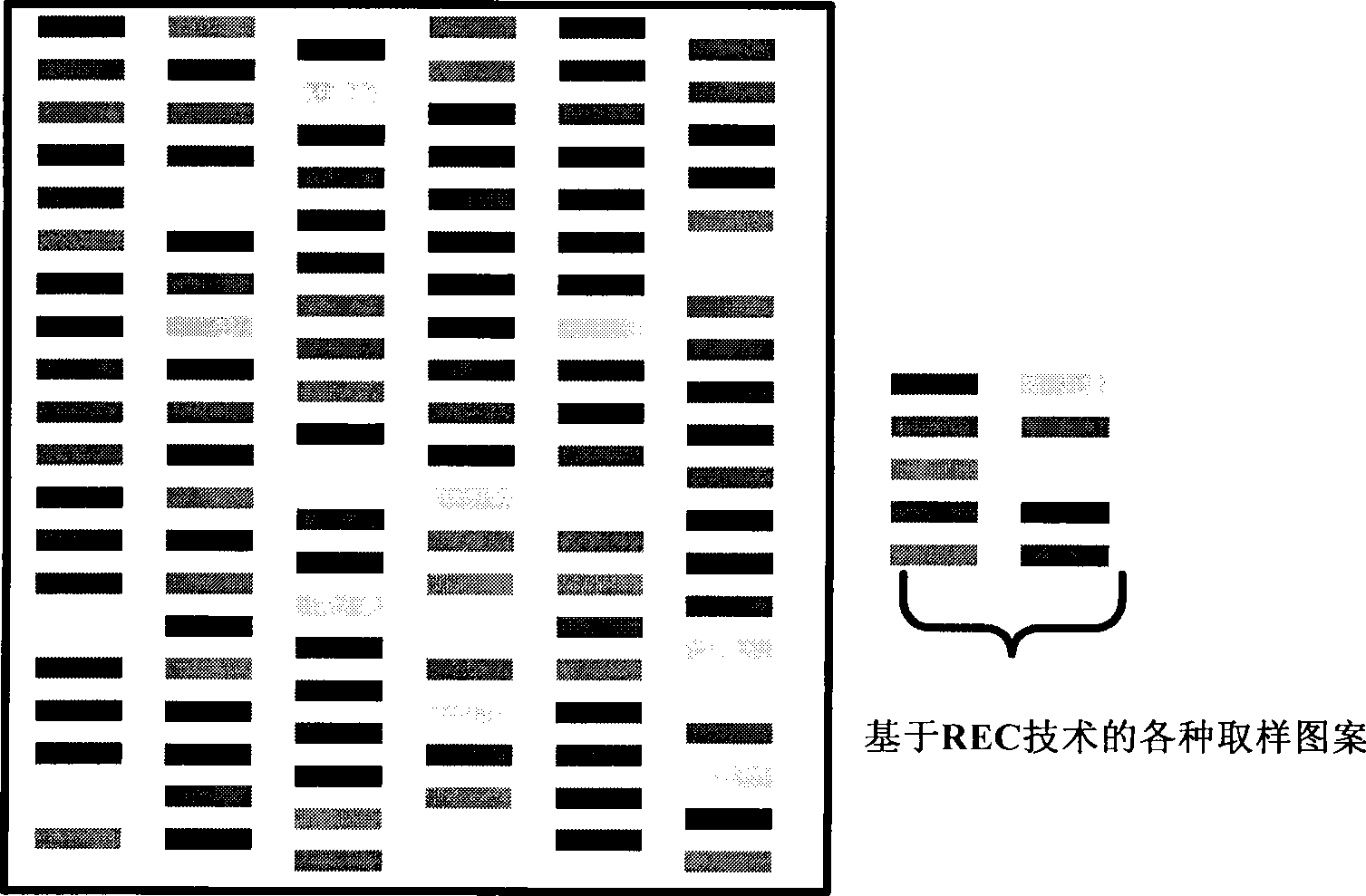
[0040] The sampled Bragg grating has multiple shadow gratings, and the wavelength interval between the shadow gratings is inversely proportional to the sampling period and the effective refractive index of the semiconductor laser waveguide. The following describes a 4-wavelength monolithic integrated DFB laser array with an operating wavelength in the ...


PUM


Abstract

Method for manufacturing a monolithic integrated semiconductor laser array, wherein each laser DFB grating structure in the array being sampling Bragg grating structure, the grating of each DFB semiconductor laser waveguide in the array is sampling Bragg grating, and the sampling Bragg grating containing equivalent grating corresponding to the common Bragg grating; the mase wavelength of the DFB semiconductor laser is determined by sampling period of the sampling structure of the sampling Bragg grating within the equivalent grating action bandwidth of the sampling Bragg grating, and it is able to change mase wavelength by changing sampling period. The sampling period is increased or decreased by mask plate with various sampling pattern, and various wavelength mases are implemented by closing in or outlying a center wavelength of the DFB laser mase wavelength, thus to implement multi-channel multi-wavelength laser array; the invention implements various complicated equivalent phase-shift with sub-micron stage accuracy, namely corresponding equivalent grating has Lambada/4 phase-shift, Lambada/8 phase-shift and a CPM structure.

Description

technical field [0001] The invention belongs to the field of optoelectronic technology, relates to distributed feedback semiconductor laser arrays, and relates to the design and manufacture of complex distributed feedback semiconductor lasers, more specifically, prepares distributed feedback (DFB) semiconductor laser arrays based on reconstruction-equivalent chirp technology method and device. Background technique [0002] With the increasing application of information optoelectronic technology in communication, detection and other fields, the requirements for monolithic integrated devices in related industries are also getting higher and higher, which is one of the commanding heights of future information technology. The use of single-chip integrated modules can provide large-capacity, small-volume, and low-cost communication core equipment. For example, the most promising emerging optical network company - Infinera of the United States, has been able to provide 10×10Gb / s s...

Claims


Application Information

Patent Timeline
IPC IPC(8): H01S5/40H01S5/12
Inventor 李静思贾凌慧陈向飞
Owner NANJING UNIV
Why Eureka
Try Eureka