Differential amplifier circuit and A/D converter

一种差动放大电路、差动放大器的技术,应用在差分放大器、放大器、模/数转换等方向,能够解决变高、速度性能恶化等问题

Inactive Publication Date: 2009-02-25
RENESAS ELECTRONICS CORP
View PDF0 Cites 7 Cited by
  • Summary
  • Abstract
  • Description
  • Claims
  • Application Information

AI Technical Summary

Problems solved by technology

As a result, there is a problem that the operation deviates from the saturation region of the NMOS transistors MN31 and MN32, and there is a high possibility of causing significant speed performance deterioration.

Method used


Image

  • Differential amplifier circuit and A/D converter
  • Differential amplifier circuit and A/D converter
  • Differential amplifier circuit and A/D converter

Examples


Embodiment approach 1

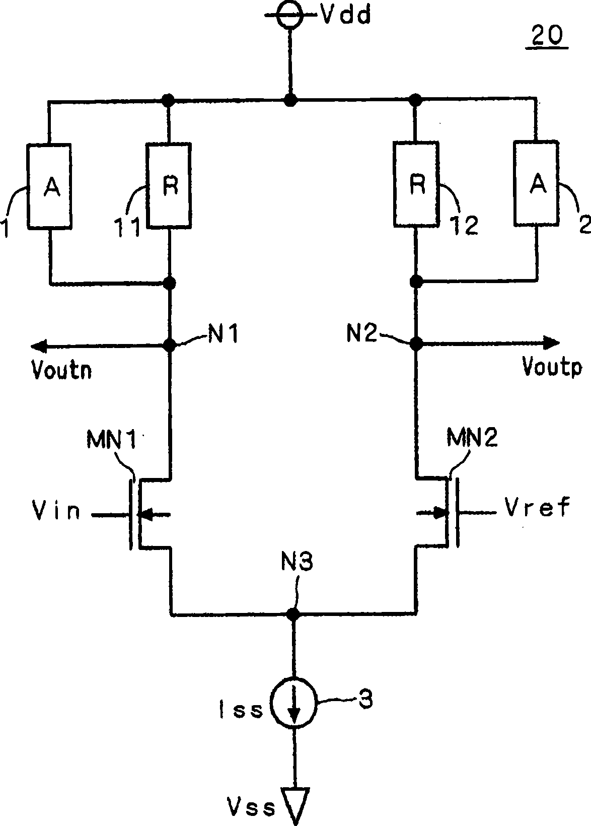
[0078] Figure 5 It is an explanatory diagram showing the configuration of a differential amplifier circuit according to Embodiment 1 of the present invention. As shown in the same figure, the differential amplifier circuit 21 according to Embodiment 1 is composed of a differential amplifier DA0 , a replica circuit 4 and a comparator 5 .

[0079] The differential amplifier DA0 has a pair of differential pair transistors (NMOS transistors MN1 and MN2 ). A constant current source 3 is provided between a node N3 that is a source common terminal of the NMOS transistors MN1 and MN2 and the ground potential Vss.

[0080] In addition, PMOS transistors MP1 and MP3 are inserted in parallel between the node N1 serving as the drain of the NMOS transistor MN1 and the power supply Vdd, and PMOS transistors are inserted in parallel between the node N2 serving as the drain of the NMOS transistor MN2 and the power supply Vdd. MP2 and MP4. In this way, the PMOS transistors MP1 to MP4 are pr...

Embodiment approach 2

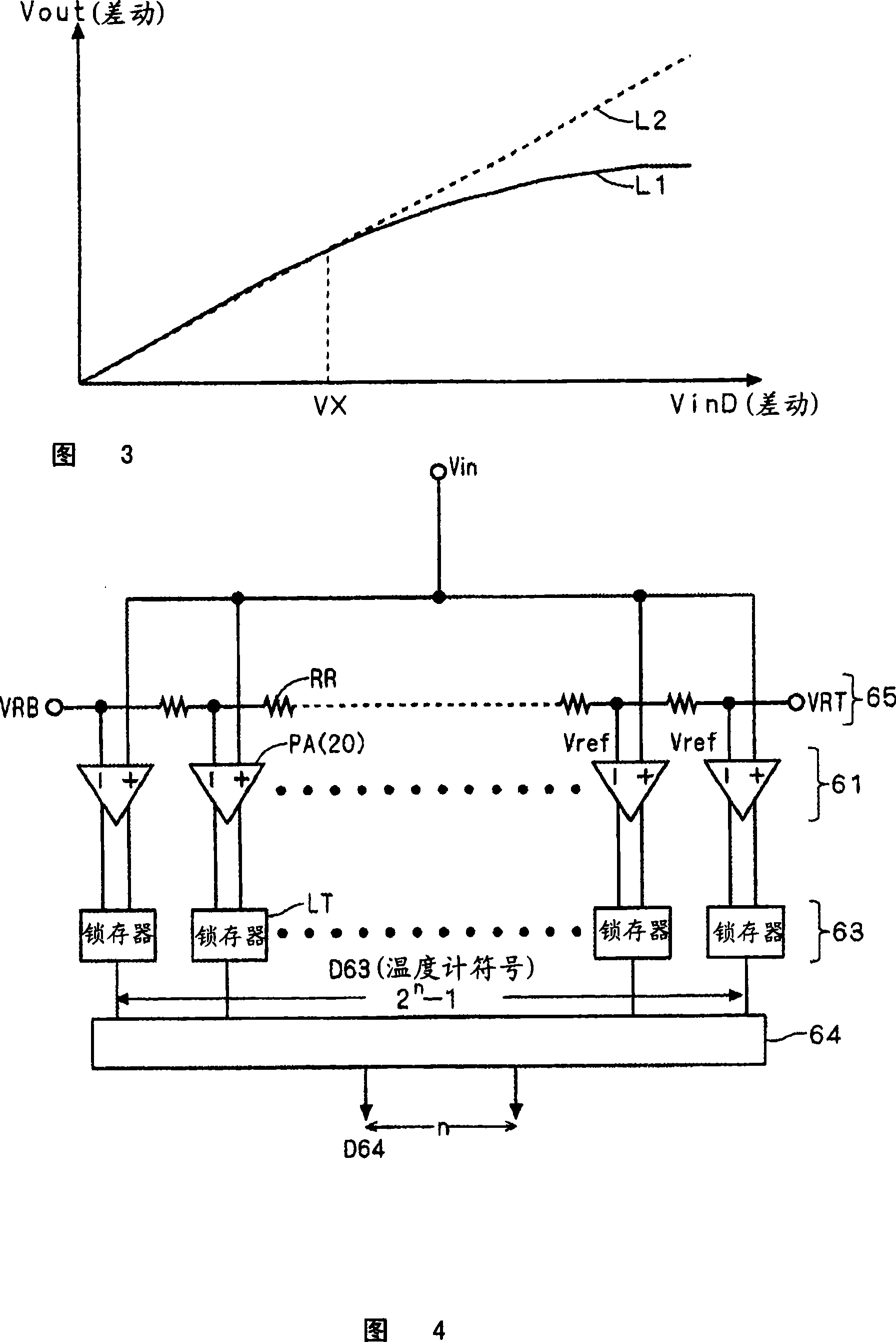
[0103] FIG. 6 is an explanatory diagram showing the configuration of a differential amplifier circuit according to Embodiment 2 of the present invention. As shown in the figure, the differential amplifier circuit 22 is composed of n (n≧2) differential amplifier stages DA1 to DAn, a replica circuit 6 and a comparator 7 .

[0104]The differential amplifier stages DA1~DAn respectively present the Figure 5 The structure equivalent to the differential amplifier DA0 of Embodiment 1 shown in . However, the reference voltages Vref input to the differential amplifier stages DA1 to DAn are reference voltages generated by a resistor ladder circuit or the like, and are set to different values ​​between the minimum reference voltage VRB and the maximum reference voltage VRT, so that The differential amplifier stages DA1 to DAn become larger (smaller) step by step.

[0105] For example, in the A / D converter shown in FIG. 4 , when the differential amplifier circuit 22 is used as the pream...

Embodiment approach 3

[0124] Figure 7 It is an explanatory diagram showing the configuration of a differential amplifier circuit according to Embodiment 3 of the present invention. As shown in the same figure, the differential amplifier circuit 23 is composed of n (n≧2) differential amplifier stages WDA1 to WDAn having a four-input structure, a replica circuit 6 and a comparator 7 .

[0125] As shown in the figure, each of the differential amplifier stages WDA1 to WDAn has two pairs of differential pair transistors (a set of NMOS transistors MN11 and MN12 and a set of NMOS transistors MN13 and MN14 ).

[0126] The constant current source 13 is set between the node N13 which is a common terminal of the sources of the NMOS transistors MN11 and MN12 (the first one and the other differential transistor) and the ground potential Vss. The constant current source 13 supplies a constant current Iss.

[0127] In addition, between the node N1 that is the drain of the NMOS transistor MN11 and the power sup...


PUM


Abstract

The present invention aims to provide a differential amplifier circuit that prevents degradation of performance and that can be overdrive recovered even if a power supply voltage is relatively small. PMOS transistors are interposed parallel to each other between a node, which is a first output part, and a power supply; and PMOS transistors are interposed in parallel to each other between a node, which is a second output part, and the power supply. Output voltages in time of a balanced state in which an input potential difference between an input voltage and a reference voltage is '0' are bothset to a reference output common voltage by a replica circuit and a comparator. The reference output common voltage of the replica circuit is set so that the potential difference between the power supply voltage and the output common voltage becomes a value lower than a threshold voltage of the diode connected PMOS transistors.

Description

technical field [0001] The present invention relates to a differential amplifier circuit constituting a comparator which is a component circuit of an A / D converter, and an A / D converter including the differential amplifier circuit. Background technique [0002] In the read channel of ODD (Optical Disc Drive: Optical Disc Drive) such as HDD (Hard Disk Drive: Hard Disk Drive) or DVD (Digtal Versatile Disk: Digital Versatile Disc), that is, a system that reads signals recorded on the disc, when digital Signal processing An A / D converter that converts analog signals into digital signals is required for signal processing (demodulation). In recent years, with the increase in reading speed and recording density in HDDs, ultra-high-speed A / D converters exceeding 1 GS / S are required. [0003] In conventional differential amplifiers (differential amplifier stages) that use a relatively high power supply voltage Vdd as an operating power supply, transistors that connect the gate and d...

Claims


Application Information

Patent Timeline
Patent Type & Authority Applications(China)
IPC IPC(8): H03F3/45H03M1/34
CPCH03F2203/45424H03F3/45183H03F2200/453H03F3/45659H03F2203/45082H03F3/45
Inventor 出口和亮三木隆博
Owner RENESAS ELECTRONICS CORP
Why Eureka
Try Eureka