
Semiconductor device and method for fabricating the same

A technology for semiconductors and high-voltage regions, which is applied in the field of semiconductor devices and their manufacturing, and can solve problems such as lowering device reliability, lowering doping concentration, and subthreshold leakage

Inactive Publication Date: 2009-03-11
DONGBU HITEK CO LTD
View PDF0 Cites 8 Cited by
  • Summary
  • Abstract
  • Description
  • Claims
  • Application Information

AI Technical Summary

Problems solved by technology

As a result, the doping concentration is reduced (S1) and anomalous sub-threshold leakage can occur in high-voltage or high-power transistor devices
In addition, the concentration of an electric field (eg, sharpening phenomenon) may cause degradation, thereby reducing device reliability

Method used


Image

  • Semiconductor device and method for fabricating the same
  • Semiconductor device and method for fabricating the same
  • Semiconductor device and method for fabricating the same

Examples


Embodiment Construction

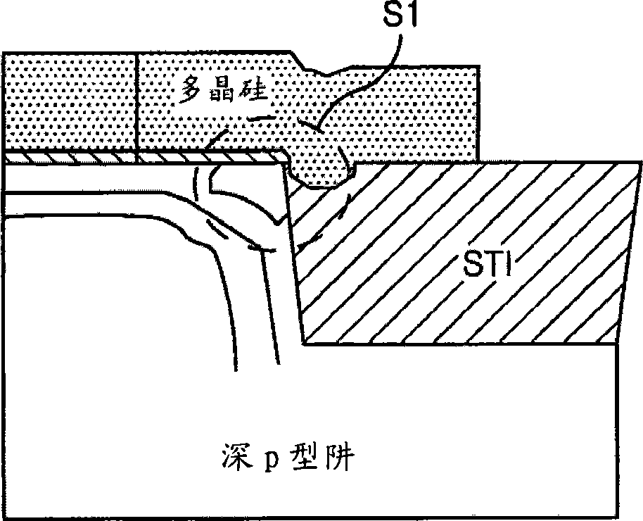
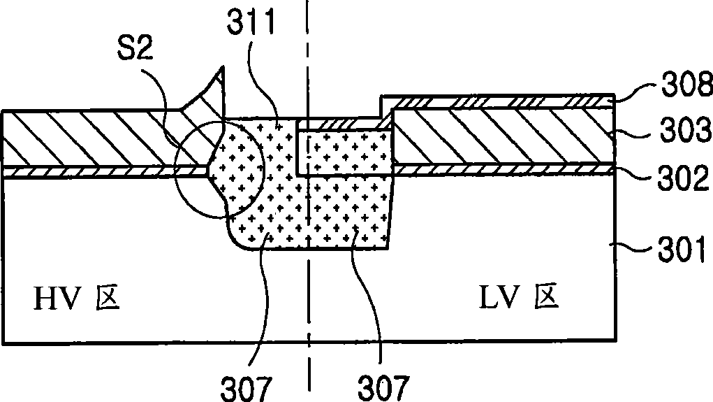
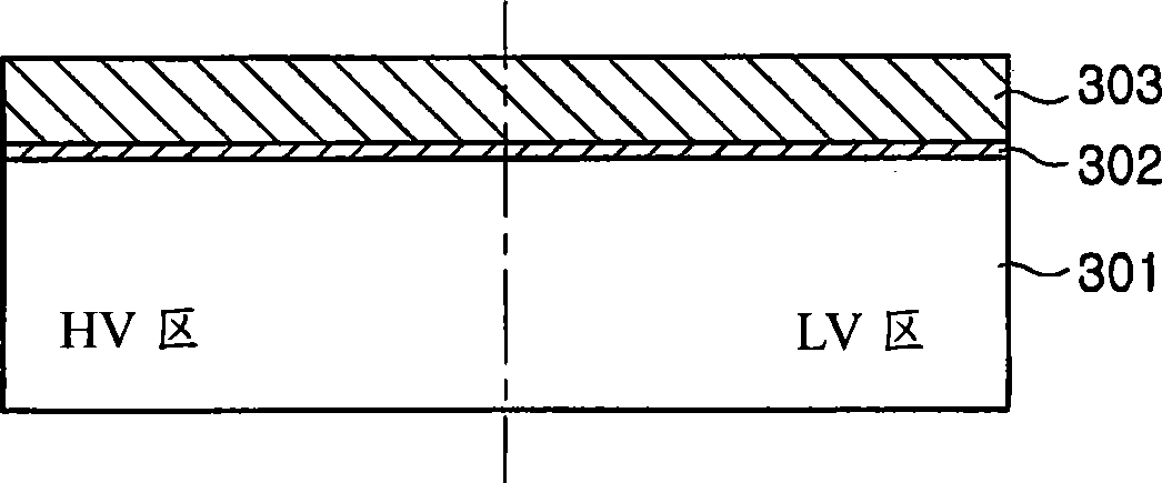
[0011] example figure 2 A structure of a semiconductor device in which an STI is formed according to an embodiment of the present invention is shown. reference example figure 2 , a pad oxide film 302 may be sequentially formed over a semiconductor substrate (P-type substrate (P-Substrate)) which may include a high voltage (hereinafter, referred to as HV) region and a low voltage (hereinafter, referred to as LV) region and nitride film 303. The pad oxide film 302 and the nitride film 303 can be selectively removed using the PR pattern 304 . The STI 305 can be formed using the removed pad oxide film 302 and nitride film 303 as an etching mask.

[0012] An oxide film 306 may be formed thereon and planarized by a planarization process. A capping layer (for example, a nitride film) 308 may be formed over the entire surface of the planarized top portion. The PR pattern 309 may be formed to open only the HV region, and then the nitride film of the HV region may be removed by a...


PUM

PropertyMeasurementUnit
Thicknessaaaaaaaaaa

Abstract

Embodiments relate to the lowered reliability of a device due to deterioration caused by the concentration of an electric field in the top corner of an STI. To solve the reliability problem, the STI top corners have a local oxidation of silicon, the top corners of the STI are rounded, and the STI steps are increased in a semiconductor device fabricated according to embodiments. Embodiments relate to an STI in high and low voltage regions of a semiconductor device which can be fabricated by providing a semiconductor substrate having a shallow trench isolation structure, a high voltage region and a low voltage region. A capping layer is formed over the entire surface of the top of the high voltage region and the low voltage region, including the shallow trench isolation structure. A photoresist pattern is formed over the top of the capping layer to expose the high voltage region, including a portion of the shallow trench isolation structure formed within the high voltage region. The capping layer of the high voltage region is removed by performing an etching process using the photoresist pattern as a mask. An oxidation process is performed on the shallow trench isolation structure top corners of the high voltage region from which the capping layer is removed. An ion implantation is then carried out. The ion implantation may be carried out by implanting boron using a tilt method.

Description

[0001] This application claims priority from Korean Patent Application No. 10-2007-0090912 (filed on September 7, 2007) based on 35 U.S.C119, the entire contents of which are hereby incorporated by reference. technical field [0002] The present invention relates to a semiconductor device, and more particularly, to a semiconductor device and a manufacturing method thereof, which can solve reliability problems of HV devices, which may arise during the manufacturing process of high voltage or high power devices In conventional STI (Shallow Trench Isolation, hereinafter, referred to as STI). Background technique [0003] As integrated circuits having various functions coexist in the same product, and semiconductor circuits become more highly integrated, there is a demand for high-voltage or high-power transistors for driving multiple voltages and currents. A thin film transistor-liquid crystal device (thin film transistor-liquid crystal device) includes a driving circuit and a ...

Claims


Application Information

Patent Timeline
IPC IPC(8): H01L21/822H01L21/762H01L21/265H01L27/04
CPCH01L21/76235H01L21/823481H01L21/823462
Inventor 崔容建
Owner DONGBU HITEK CO LTD
Features
  • Generate Ideas
  • Intellectual Property
  • Life Sciences
  • Materials
  • Tech Scout
  • Unparalleled Data Quality
  • Higher Quality Content
  • 60% Fewer Hallucinations
Learn More