Routing node microstructure for on-chip network

A network-on-chip and microstructure technology, applied in data exchange network, data exchange details, digital transmission system, etc., can solve problems such as component communication bottleneck effect, transistor quantity limitation, SoC chip performance limitation, etc.

Inactive Publication Date: 2009-03-11
UNIV OF ELECTRONICS SCI & TECH OF CHINA
View PDF0 Cites 36 Cited by
  • Summary
  • Abstract
  • Description
  • Claims
  • Application Information

AI Technical Summary

Problems solved by technology

[0005] 1. The number of components that can be effectively connected by the bus is small, and as the number of components connected by the bus increases, the conflicts between the components will also increase, which will The complexity of the SoC is limited;
[0006] 2. As the number of components connected to the bus increases, the length of the bus will also increase, but in SoC design, a long global bus will cause components in the SoC The bottleneck effect of communication, thereby reducing communication efficiency and even causing congestion;
[0007]Third. To connect many components on the same bus, all components are required to have a standard and unified bus interface, which will bring problems to the design of each component. additional overhead;
[0008] 4. The communication bottleneck caused by the bus structure will also limit the size of the SoC. Since it cannot provide an efficient communication mode, the number of transistors in the chip that can be used is limited. Limits, resulting in SoC chip performance is limited
[0009]5. Since there is a single bus that connects the various components in the SoC, when expanding, it is necessary to design an interface that can be used for the bus for the components that need to be expanded, and The interface of each component must be unified, which reduces the design flexibility and scalability of SoC

Method used


Image

  • Routing node microstructure for on-chip network
  • Routing node microstructure for on-chip network
  • Routing node microstructure for on-chip network

Examples


Embodiment Construction

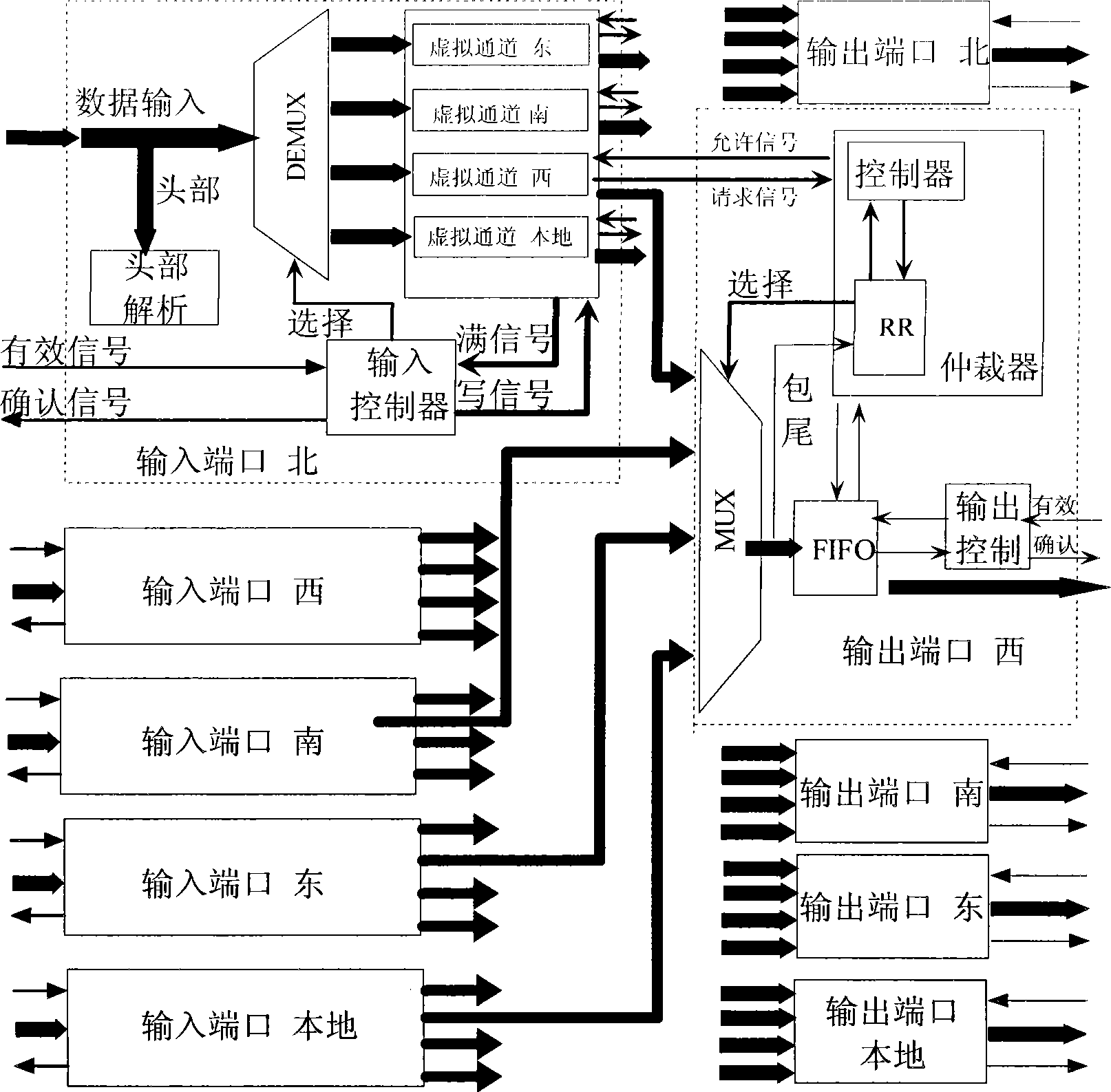
[0063] Hereinafter, the present invention will be specifically described by taking an input module and an output module composed of standard 5 output ports and 5 input ports as an example.

[0064] In terms of hardware, the input module is composed of 5 input ports, which respectively represent 5 directions of east, south, west, north and local, and the local direction is connected to the local processor.

[0065] figure 1 The dotted line in the middle indicates the structural diagram of the north-to-west transmission of the input port to the west of the output port, and the transmission between other ports is the same as figure 1 The dotted line part has the same structure.

[0066] Such as figure 1 As shown, in the present invention, when a data packet is to be transmitted from the upper-level node to the current node, the header flit carrying routing information of the data packet is first sent to the current node as a request signal. After the current node receives t...


PUM


Abstract

The invention discloses a route node microstructure of a network on chip, which comprises a head decode module, an input buffer module, an input control module, an output arbitration module, an output buffer module and an output control module. The head decode module performs the head analysis to data entering the route node from the upper route node, and inputs the data to the input buffer module; the input buffer module is used for the temporary storage of the data, and outputs the data to the output arbitration module under the action of the input control module. After the data enters the output arbitration module, the output arbitration module determines whether outputting the data to the output buffer module according to the state of the input control module, and the output arbitration module controls the whole output link so as to realize that the data is transmitted to the next route node. Through the route node microstructure of the invention, the data transmission among the route nodes of the network on chip can be realized, and the transmission efficiency can be greatly improved.

Description

technical field [0001] The invention relates to a routing node microstructure, in particular to a routing node microstructure of an on-chip network. Background technique [0002] With the development of electronic technology, complex SoC has received more and more attention. Under the current technical conditions, it is possible to integrate more than one billion gates on a single chip, which is the physical basis required by complex SoCs; at the same time, its wide range of applications has greatly increased the market demand for complex SoCs. There are many application fields of complex SoC, from security system, control system, personal health system, to mainstream consumer products, such as multimedia processing, personal communication, personal computing, entertainment, video / image and so on. In fact, most of the current dedicated ICs for these applications already have a high level of complexity. However, with the deepening of scientific research and implementation o...

Claims


Application Information

Patent Timeline
Patent Type & Authority Applications(China)
IPC IPC(8): H04L12/02H04L12/56H04L12/701
Inventor 武畅李玉柏李桓柴松杨中明王坚
Owner UNIV OF ELECTRONICS SCI & TECH OF CHINA
Why Eureka
Try Eureka