Plasma display panel and imaging device using the same

A display panel and plasma technology, which is applied to alternating current plasma display panels, identification devices, static indicators, etc., can solve the problem that the deterioration of address discharge delay cannot be suppressed over time, the deterioration of address discharge delay cannot be improved, and the Problems such as floating electrodes, etc., to achieve the effect of improving address discharge delay, improving deterioration over time, and low power consumption

Inactive Publication Date: 2009-03-25
HITACHI CONSUMER ELECTRONICS CORP
View PDF5 Cites 2 Cited by
  • Summary
  • Abstract
  • Description
  • Claims
  • Application Information

AI Technical Summary

Problems solved by technology

However, in this structure, in order to assist the sustain discharge, the floating electrodes are arranged across the center of the discharge cell, so the MgO surface on the floating electrodes caused by the sustain discharge deteriorates, and the delay of the address discharge cannot be suppressed. time deterioration
In addition, as shown in Patent Document 3, even if a floating electrode is used in the portion facing the barrier rib, the deterioration of the address discharge delay cannot be improved.
In addition, as shown in Patent Document 4 and Patent Document 5, even if the area of ​​the sustain discharge electrode used as the scan electrode and the address electrode is larger than the area of ​​the sustain discharge electrode not used as the scan electrode and the address electrode, Also because the floating electrodes are not arranged in the appropriate place, the effect of the floating electrodes cannot be obtained

Method used


Image

  • Plasma display panel and imaging device using the same
  • Plasma display panel and imaging device using the same
  • Plasma display panel and imaging device using the same

Examples


Embodiment 1

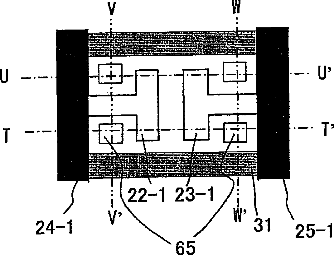
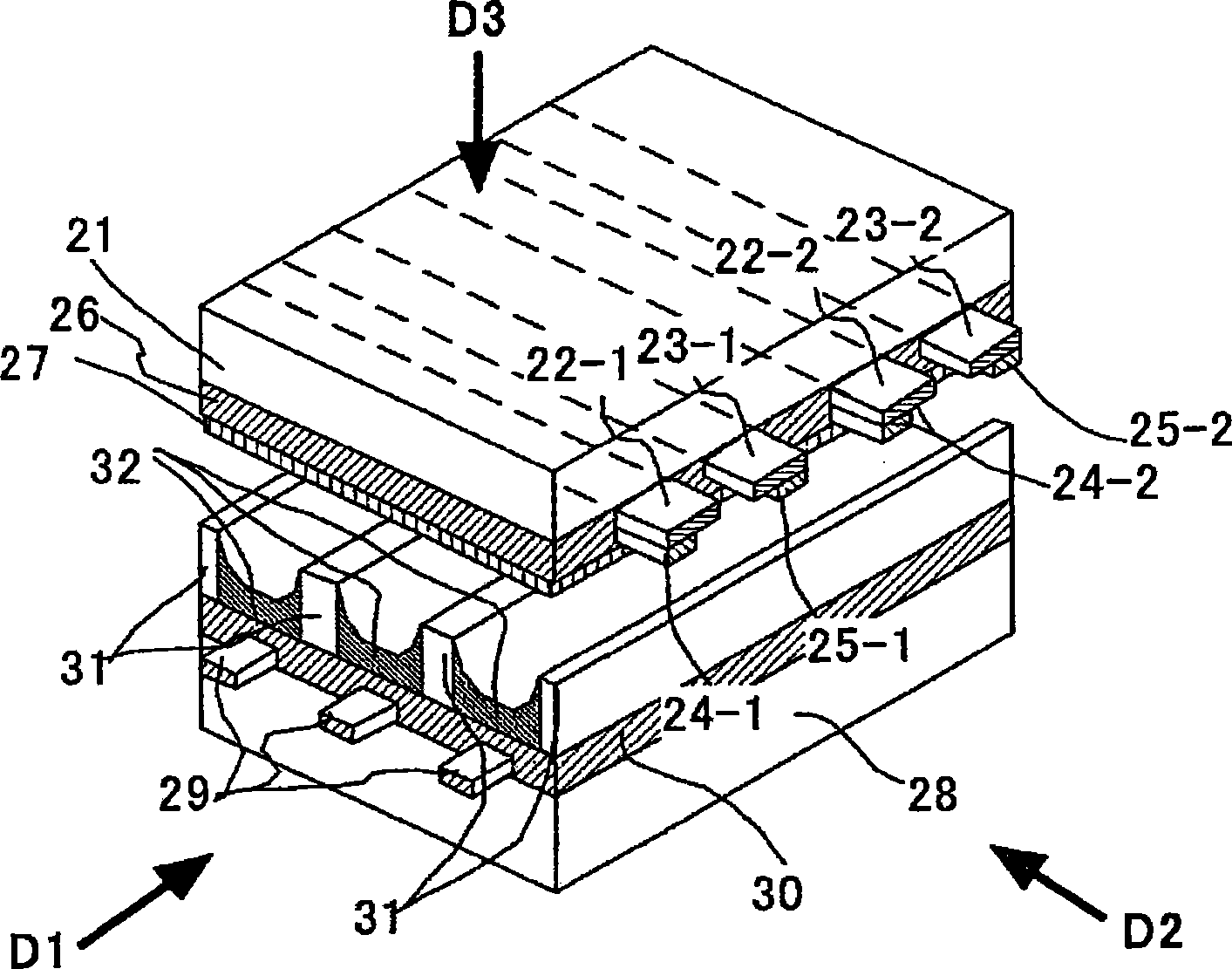
[0107] figure 1 It shows an example of embodiment related to this invention, and is a figure which shows the electrode structure of one discharge cell. Such as figure 1 As shown in , the electrodes not connected to the circuit are arranged in the discharge cells. This will be referred to as a floating electrode 65 below. The floating electrode also contains only ground (earth) potential. Make a 42-type PDP with this electrode shape, and place Figure 8 A PDP having an electrode structure shown in (A) was evaluated as a comparison object. These PDPs were fabricated with a dielectric layer 26 thickness of 32 microns. In addition, make the X electrode 22-1 and the X bus electrode 24-1, and the closest shortest distance to the floating electrode 65 on the X electrode side is 16 microns. The closest shortest distance of the floating electrodes 65 on the electrode side is 16 μm for the PDP.

[0108] The results are shown in Table 1. The address discharge delay shown in the...

Embodiment 2

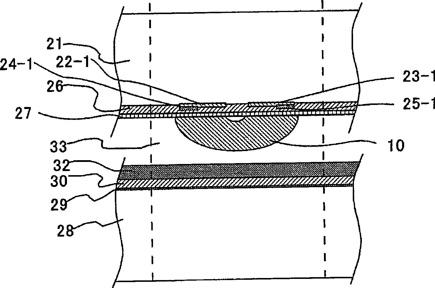
[0116] Figure 10 It shows an example of an embodiment of the present invention, and is a diagram showing an electrode structure of one discharge cell. As shown, electrodes insulated from circuits are arranged to float within the discharge cells. The state of the discharge trace portion 62 after the 1000-hour, 70 kHz life test is shown. Figure 10 (A) is a PDP with h1 of 32 microns, Figure 10 (B) is a case of a PDP in which h1 is 15 micrometers.

[0117] As can be seen from the figure, when h1 is 32 micrometers, the discharge trace portion 62 is dyed from the electrode. On the other hand, when h1 is 15 micrometers, the discharge trace portion 62 is substantially overlapped on the electrode. Thus, even if the electrode shapes are the same, if h1 is different, the reason why the shape of the discharge trace portion is different is as follows.

[0118] When a voltage is applied to the X electrode and the Y electrode, a potential is formed in the discharge space through the ...

Embodiment 3

[0129] Figure 16 It shows an example of an embodiment of the present invention, and is a diagram showing an electrode structure of one discharge cell. In this electrode structure, the address electrodes are arranged such that the overlap of the address electrodes 35 facing the Y electrodes 23-1 and the floating electrodes 65 is increased. Figure 16 (A) is in figure 1 The structure of addressing electrodes is added in . A 42-type PDP having this electrode configuration was produced. The dielectric layer 26 has a thickness of 25 microns. A life test of 1000 hours at 70 kHz was performed on this PDP. As a result, the number of seed electrons M after the life test 0 becomes 7.3×10 5 . on the other hand, Figure 15 The structure shown in (B) is a comparative object, and address electrodes are formed so that the address electrodes do not overlap with the floating electrodes 65 on the X electrode 22-1 side. The number of seed electrons M after the life test in this electr...


PUM


Abstract

There is provided a PDP and an image display apparatus equipped with the same, in which the deterioration in the address discharge timelag with age is suppressed, which is bright, has guaranteed life, can stably be driven, is of low power consumption, high definition, and high image quality. There is provided a pair of sustaining discharge electrodes on the front substrate extending in a row direction for forming a display line, a floating electrode not connected to an external electrode is arranged on the same substrate as the pair of sustaining discharge electrode so as not to pass through a center line extending in a column direction and dividing the discharge cell into two equal parts, thereby intensifying the local potential of an area of the MgO surface not influenced by the sputtering by the sustaining discharge in the address discharge, promoting the electron emission from this area, and suppressing the deterioration of the address discharge timelag.

Description

technical field [0001] The present invention relates to a plasma display panel (Plasma Display Panel: hereinafter also referred to as a plasma panel or PDP), and more particularly to a structure of a plasma panel including a PDP capable of reducing address discharge delay and its deterioration and achieving high image quality and A drive device for a plasma display device. Background technique [0002] In recent years, plasma display devices have been expected as large and thin color display devices. In particular, an alternating current (AC) in-plane discharge type PDP that generates display discharge between electrodes provided on the same substrate and is driven by alternating current is the most practical method due to its simple structure and high reliability. Next, an embodiment of a conventional AC in-plane discharge type PDP will be described. [0003] figure 2 It is an example of an exploded perspective view showing part of the structure of a general AC surface d...

Claims


Application Information

Patent Timeline
Patent Type & Authority Applications(China)
IPC IPC(8): H01J17/49H01J17/04H01J17/02G09F9/313G09G3/28H01J11/22H01J11/24H01J11/32H01J11/34
CPCG09G2320/043H01J11/30G09G3/293G09G3/2986H01J11/12H01J11/38
Inventor 植村典弘信木俊一郎何希伦铃木敬三椎木正敏
Owner HITACHI CONSUMER ELECTRONICS CORP
Why Eureka
Try Eureka