Electroluminescent device

An electroluminescence device and a luminescence technology, applied in the field of manufacturing conversion elements, can solve problems such as low luminous efficiency

Active Publication Date: 2009-04-08
LUMILEDS HLDG BV
View PDF1 Cites 19 Cited by
  • Summary
  • Abstract
  • Description
  • Claims
  • Application Information

AI Technical Summary

Problems solved by technology

However, the favorable scattering properties of such ceramic materials for producing a homogeneous col

Method used


Image

  • Electroluminescent device
  • Electroluminescent device
  • Electroluminescent device

Examples


Embodiment Construction

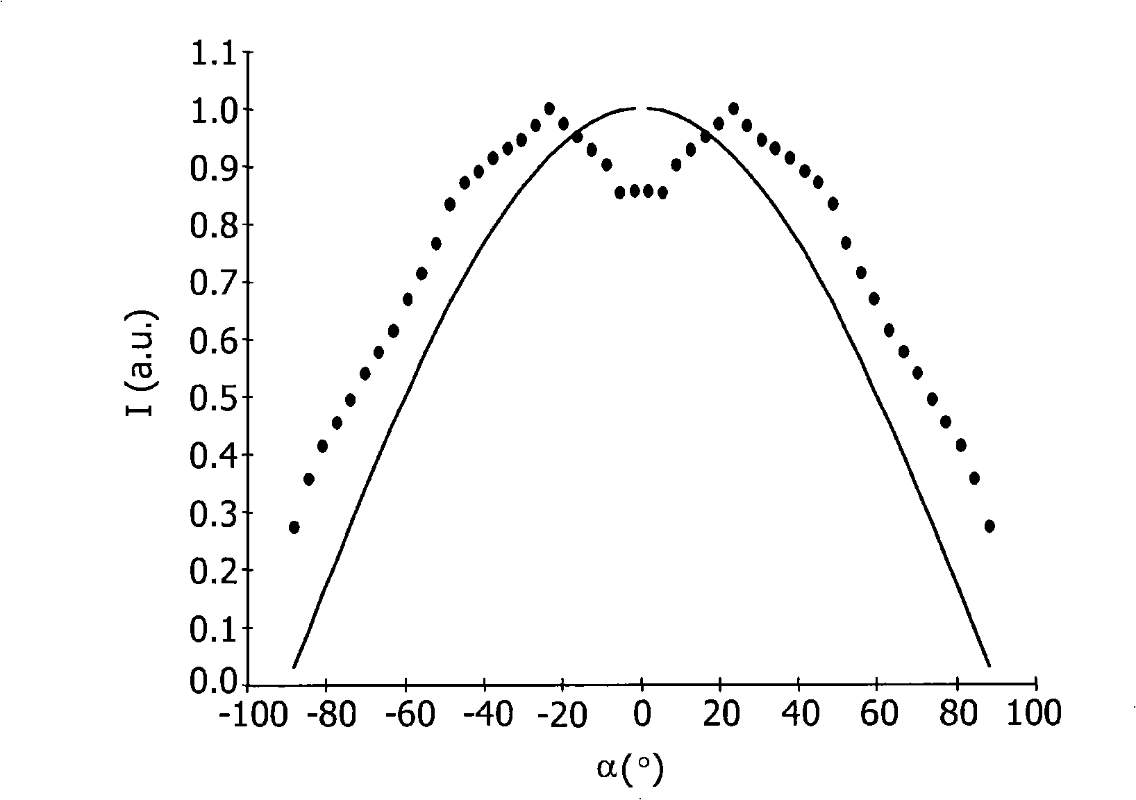
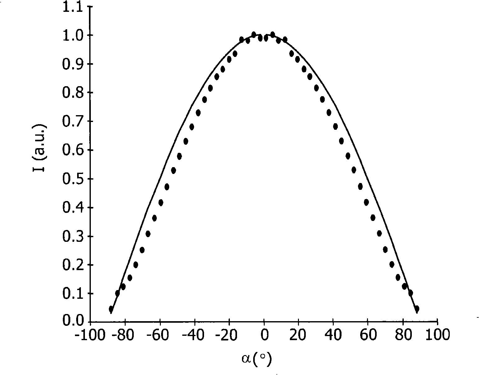
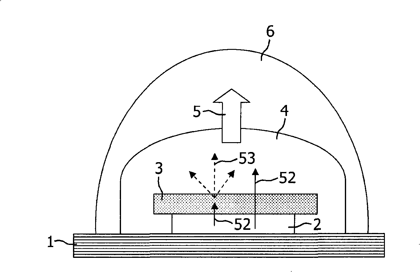
[0042] figure 2 An embodiment of a luminescent device according to the invention is schematically shown with a substrate 1 and an electroluminescent light source 2 applied on the substrate 1 for emitting primary radiation 52 and arranged on the electroluminescent light source 2 The conversion element 3 on the top is used for at least partially absorbing the primary radiation 52 and emitting the secondary radiation 53 . The electroluminescent light source 2 comprises an electroluminescent layer structure applied on the substrate 1, which structure has at least one organic or inorganic electroluminescent layer, which layer is arranged between two electrodes. Here, primary radiation is emitted by a transparent electrode (top emitter) on the side facing away from the substrate, and is reflected by the electrode facing the substrate 1 and / or the substrate 1 (eg aluminium). Here, the luminous means can also comprise a planar arrangement of several electroluminescent light sources,...


PUM


Abstract

A conversion element (3) comprising a ceramic material (31) with a multiplicity of pores (32) provided for at least the partial absorption of at least one primary radiation (52) and for transforming the primary radiation (52) into at least one secondary radiation (53), wherein the conversion element (3) has a density greater than or equal to 97% of the theoretical solid-state density of the ceramic material (31), and the pores (32) in the conversion element (3) have a diameter substantially between 200 nm and 5000 nm.

Description

technical field [0001] The present invention relates to high-efficiency electroluminescent devices having a radiation pattern similar to a cosine radiation pattern, comprising a conversion element for converting light, and to a method of manufacturing the conversion element Background technique [0002] Phosphor-converted electroluminescent devices (pcLEDs) having an electroluminescent light source (LED) and a light-converting phosphor layer, usually a phosphor powder layer or a polycrystalline phosphor layer, are known. With such pcLEDs, at least part of the primary radiation emitted by the LED is absorbed by a phosphor layer (conversion element) arranged on the LED and re-emitted as longer wavelength secondary radiation. This process is also known as color or light conversion. Depending on the application, the primary radiation is completely converted into secondary radiation or, in the case of partial conversion, light of a different color (eg white light) can be produce...

Claims


Application Information

Patent Timeline
IPC IPC(8): C09K11/77H01L33/50
CPCC04B35/645C04B2235/3229C04B2235/3225C04B35/16C04B35/6265C04B2235/663C04B2235/658C09K11/7774H01L33/502C04B35/6261C04B2235/652C04B2235/608C04B2235/3217C04B2235/77C04B2235/3215C04B2235/3224C04B38/0074C04B2235/5445C04B2235/3208C04B2235/764C04B35/44C04B38/0054C04B2111/807C04B2235/3213H01L2924/0002Y10T428/249953H01L2924/00
Inventor P·斯米特H·-H·贝克特尔W·巴塞尔特B·-S·施赖恩马彻
Owner LUMILEDS HLDG BV
Why Eureka
Try Eureka