Display module

A display and display panel technology, applied to static indicators, instruments, electric solid devices, etc., can solve problems such as increased manufacturing costs, short circuits, and reduced yields

Inactive Publication Date: 2009-04-15
CHUNGHWA PICTURE TUBES LTD
View PDF0 Cites 8 Cited by
  • Summary
  • Abstract
  • Description
  • Claims
  • Application Information

AI Technical Summary

Problems solved by technology

[0005] However, in the current manufacturing process of liquid crystal silicon-based display modules, during the soldering step, directly soldering tin on the surface of ITO will cause the silicon wafer to conduct with the glass substrate due to the overflow of sold...

Method used


Image

  • Display module
  • Display module
  • Display module

Examples


Embodiment 1

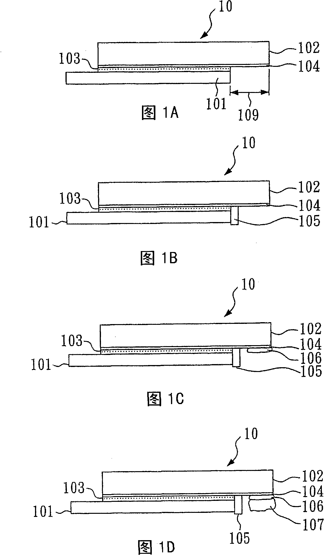
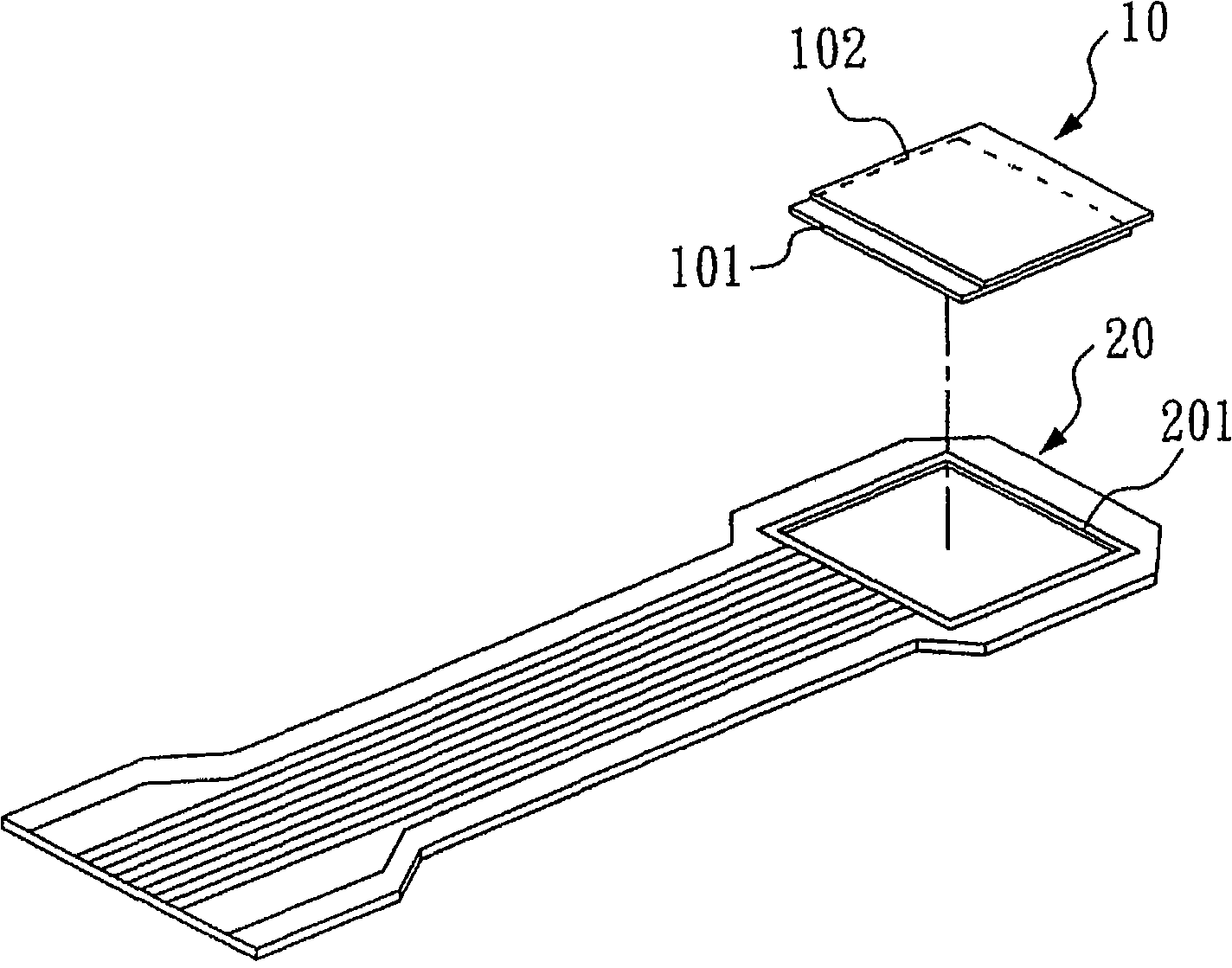
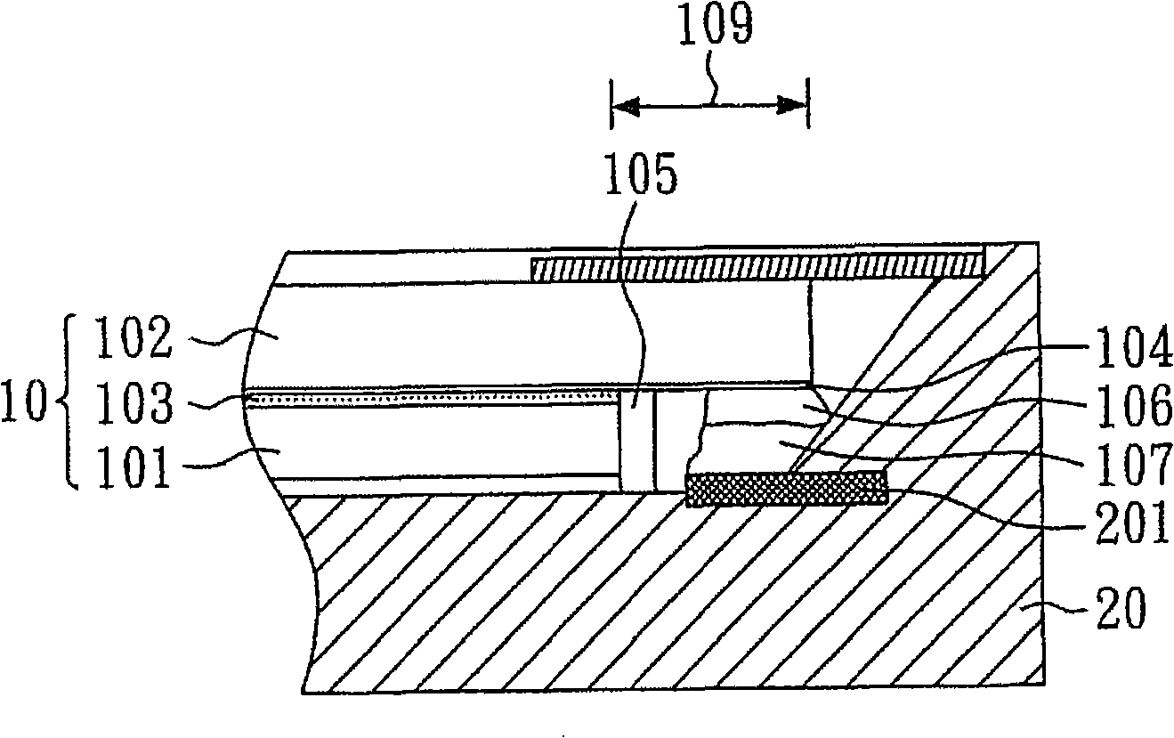
[0029] Such as image 3 Shown is a cross-sectional view of the structure of the display module of this embodiment, which includes: a display panel 10 , a transparent electrode layer 104 , a casing 20 , a conductive glue 107 , a solder layer 106 , and an insulating glue 105 . The display panel 10 includes a lower substrate 101 , an upper substrate 102 , and a liquid crystal layer 103 . Wherein, the upper substrate 101 and the lower substrate are disposed opposite to each other, and the liquid crystal layer 103 is disposed between the upper substrate 101 and the lower substrate 102 . Moreover, the display panel 10 has a dislocation portion 109 , and the transparent electrode layer 104 is disposed on the upper substrate 102 and extends to the dislocation portion 109 . On the other hand, the housing 20 has a conductive line 201 . In addition, the conductive glue 107 is connected to the transparent electrode layer 104 and the conductive circuit 201 . The solder layer 106 is form...

Embodiment 2

[0036] Please refer to Figure 4 to Figure 5 , is the flow chart of manufacturing the display module of this embodiment. The manufacturing method of this embodiment is substantially the same as that of Embodiment 1, but the difference is that, as shown in FIG. 4D : after the step of coating the solder layer 106, the solder resist layer 108 is applied between the insulating glue 105 and the solder layer 106 . Next, the solder resist layer 108 (not shown) is hardened. In this embodiment, the method of hardening the solder resist layer 108 is thermal hardening. The solder resist layer 108 in this embodiment has the effect of strengthening the blocking of overflowing solder paste, and can further strengthen the effect of preventing the upper substrate 102 from being electrically connected to the lower substrate 101 .

[0037] The structure of the display module of this embodiment is substantially the same as that of Embodiment 1, but the structure of the display module of this em...


PUM


Abstract

The invention provides a displayer module which comprises a display panel, a transparency electrode layer, conducting resin, a soldering tin layer and insulating cement. The invention also provides a method for manufacturing the displayer module, and the method comprises: the display panel, coating insulating cement, hardening insulating cement, coating soldering tin layer and coating conducting resin are provided; a shell which is provided with a conductive circuit, a combined display panel and shell, a heat bonding soldering tin layer and the conducting resin are provided. In the invention, the insulating cement is used for preventing the soldering tin and the conducting resin from overflowing. Therefore, the insulating cement of the displayer module of the invention can prevent conductance between an upper base plate and a lower base plate.

Description

technical field [0001] The invention relates to a display module, in particular to a display module with low conductivity of upper and lower substrates. Background technique [0002] In recent years, LCDs have gradually been widely used in daily life, such as LCD TVs, notebook computers, LCD screens of desktop computers, and LCD projectors. Generally speaking, LCD projectors are one of the important tools for large-scale displays, and the core of LCD projectors lies in the optical engine for projection. panel. [0003] The above-mentioned liquid crystal panel mainly adopts a liquid crystal on silicon (LCoS) panel, which is a silicon substrate that integrates a liquid crystal panel into a silicon substrate that can be manufactured by an integrated circuit. Generally speaking, in the manufacturing method of the liquid crystal silicon-based panel, transistors and reflective layers are firstly formed on the silicon wafer, then a glass substrate is bonded, and finally liquid cr...

Claims


Application Information

Patent Timeline
IPC IPC(8): G02F1/133G02F1/1362H01L27/32
Inventor 王君铭李怀安陈昆泓陈玉仙莫启能许心仪
Owner CHUNGHWA PICTURE TUBES LTD
Why Eureka
Try Eureka