
Radio frequency identification label chip data receiving synchronous method
A radio frequency identification tag and data technology, applied in instruments, inductive record carriers, computer parts, etc., can solve problems such as data sampling errors, complex timing problems, inability to generate clock edges, etc., and achieve simple structure and strong adaptability. Effect
Patent Information
- Authority / Receiving Office
- CN · China
- Current Assignee / Owner
- Publication Date
- 2009-04-15
- Estimated Expiration
- Not applicable · inactive patent
Smart Images
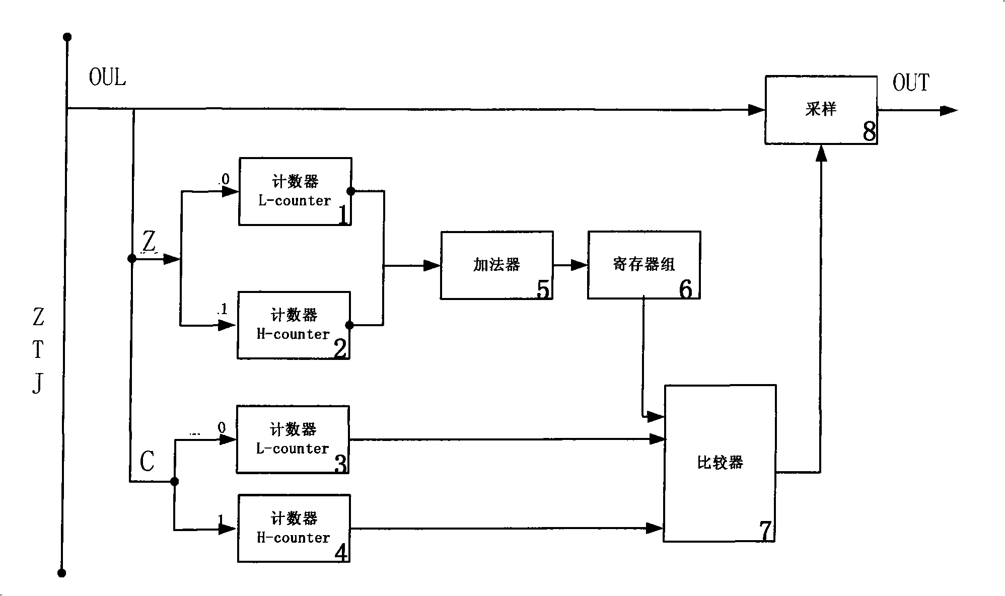
Figure 1 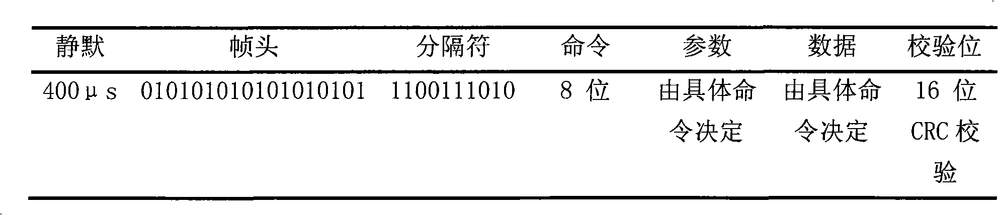
Figure 2 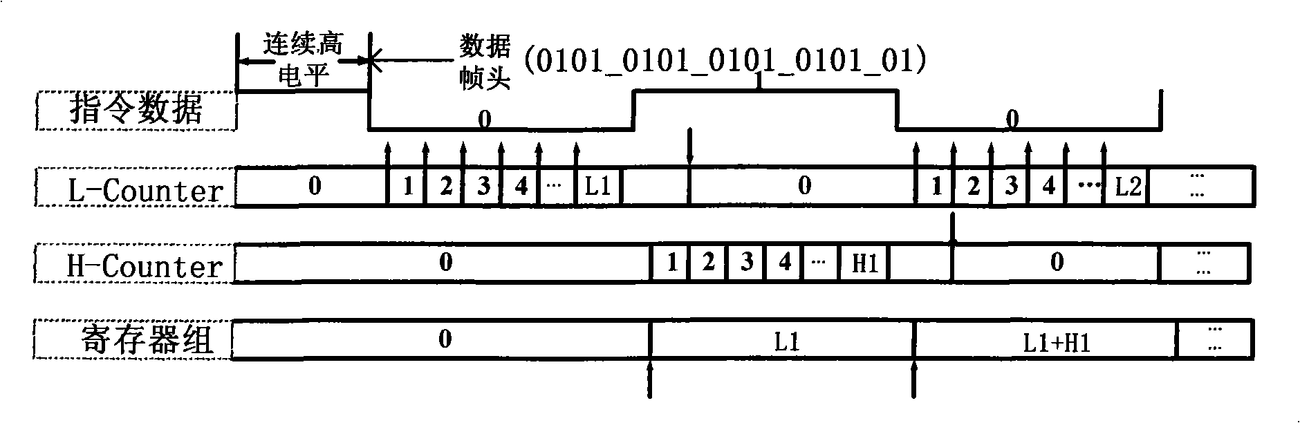
Figure 3
Abstract
Description
technical field
[0001] The invention relates to a method for synchronizing data reception of an identification tag chip. In particular, it relates to a radio frequency identification tag chip data reception synchronization method with strong adaptability to the low-stability on-chip clock. Background technique
[0002] The radio frequency identification (RFID) system consists of three parts: a radio frequency tag (Tag), a card reader (Reader) and a data management system. A radio frequency tag chip usually consists of an analog front-end circuit, a digital processing unit and a memory.
[0003] For passive RFID tags, the tag first waits for the reader to issue a command, and then responds. In this case, the tag needs to recover the data modulated and encoded by the reader. Since the operation of the card reader and the tag adopts independent clock sources, the two are in a completely asynchronous clock domain. In order to correctly sample the relevant commands, the tag m...
Examples
Embodiment Construction
[0041] The radio frequency identification tag chip data reception synchronization method of the present invention will be described in detail below in conjunction with specific embodiments and accompanying drawings.
[0042] The radio frequency identification tag chip data reception synchronization method of the present invention is to adopt two counters (H-counter and L-counter) respectively to comply with the high level 1 and the low level in the instruction format of the ISO / IEC 18000-6 Type B agreement. The length of flat 0 is counted, and an adder matching the number of counter digits is used for cumulative operation, and the synchronous count value is temporarily stored in the register group. When sampling, the comparator is used to compare the count value with the accumulated and divided operation. The base reference value is compared to give the correct sampling clock edge.
[0043] Specific as figure 1 As shown, the first counter 1 is used to receive the low-level da...