Semiconductor device and method of processing the same
A manufacturing method and semiconductor technology, applied in the fields of semiconductor/solid-state device manufacturing, semiconductor devices, electrical components, etc., can solve the problems of difficult to configure superstructure, and achieve the effect of uniform expansion and increase of impurity concentration.
- Summary
- Abstract
- Description
- Claims
- Application Information
AI Technical Summary
Problems solved by technology
Method used
Image

Examples
Embodiment Construction
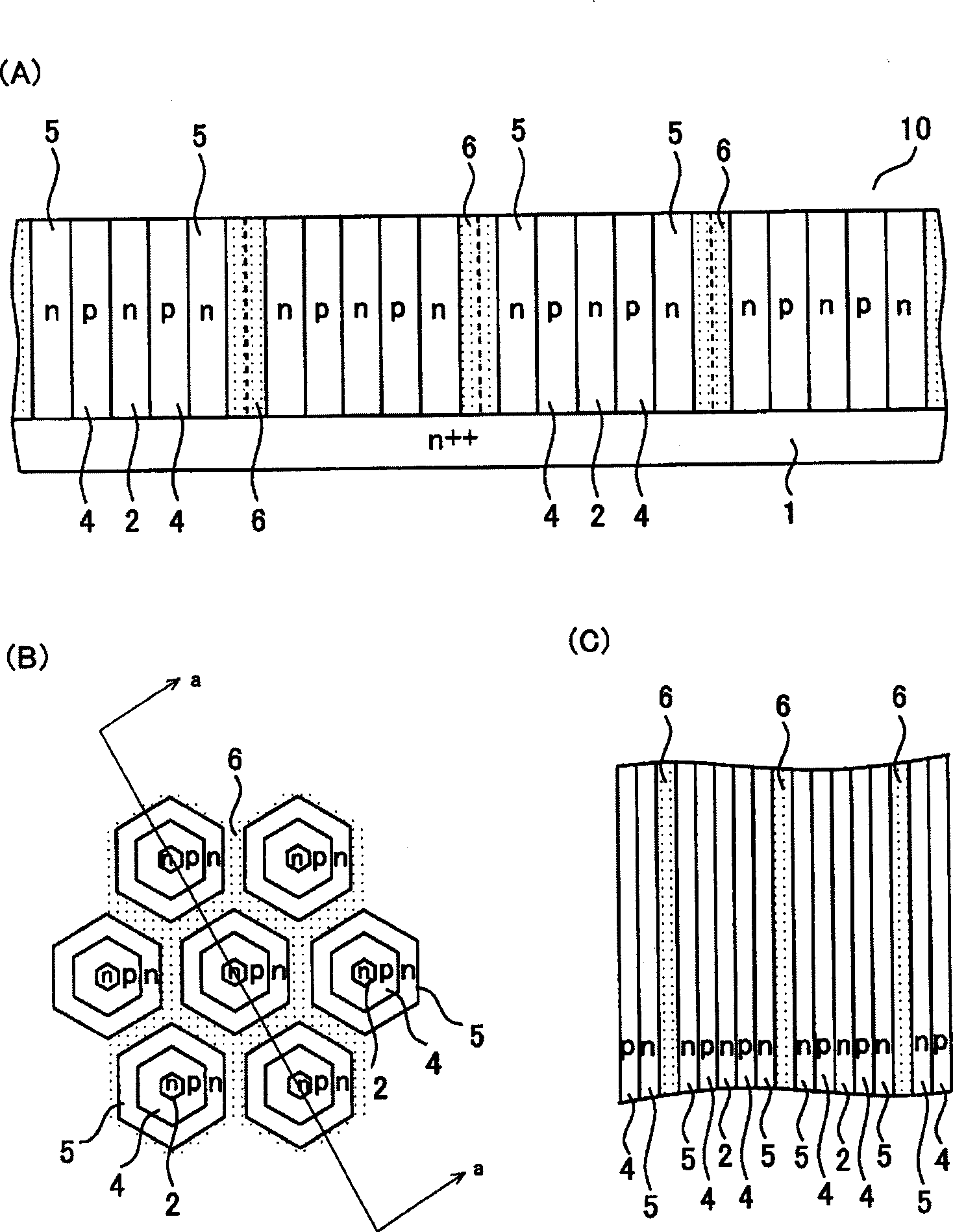
[0047] refer to Figure 1 to Figure 9 , the embodiment of the present invention will be described in detail by taking the case where the semiconductor substrate is an n-type silicon semiconductor substrate as an example.
[0048] The semiconductor wafer of the present invention is composed of a conductive semiconductor substrate, a first semiconductor layer, a second semiconductor layer, a third semiconductor layer and an insulating layer, and a plurality of pn junctions are arranged in a direction perpendicular to the surface of the semiconductor wafer.
[0049] figure 1 It is a figure which shows an example of the semiconductor wafer 10 of this embodiment, figure 1 (A) is a sectional view, figure 1 (B) and figure 1 (C) is a diagram showing a pattern of one main surface of the semiconductor wafer 10 . in addition, figure 1 (A) is figure 1 (B) A-a line sectional view.
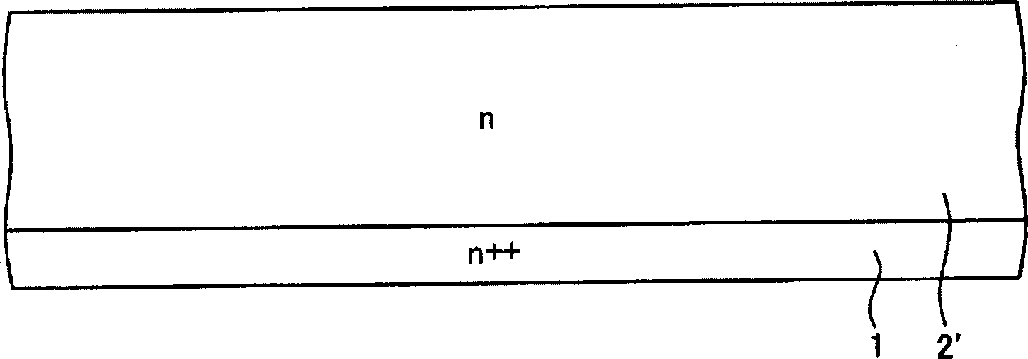
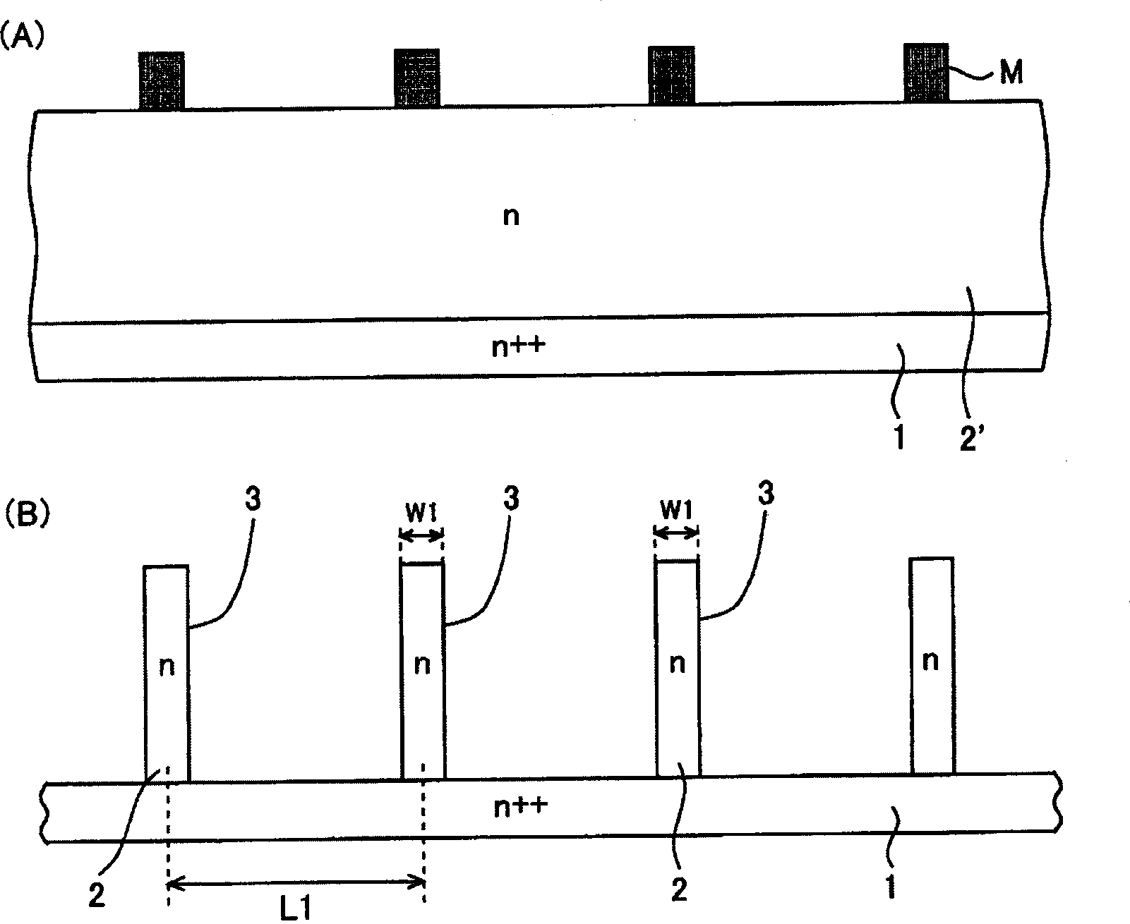
[0050] refer to figure 1 (A), a conductive type semiconductor substrate 1 is, for example, an...
PUM
 Abstract
Description
Claims
Application Information
 - R&D
- Intellectual Property
- Life Sciences
- Materials
- Tech Scout
- Unparalleled Data Quality
- Higher Quality Content
- 60% Fewer Hallucinations
Browse by: Latest US Patents, China's latest patents, Technical Efficacy Thesaurus, Application Domain, Technology Topic, Popular Technical Reports.
© 2025 PatSnap. All rights reserved.Legal|Privacy policy|Modern Slavery Act Transparency Statement|Sitemap|About US| Contact US: help@patsnap.com